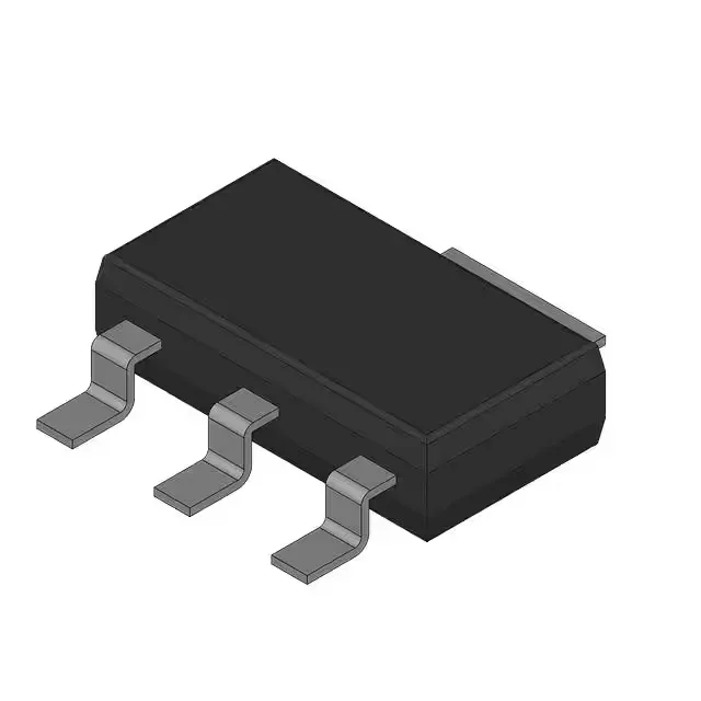
Infineon Technologies BSP320SL6327

Infineon BSP320SL6327 SIPMOS N-Channel MOSFET, 60 V, 2.9 A

MPNBSP320SL6327
End of Life

Infineon SIPMOS® N-Channel MOSFET, 60 V drain-source, 2.9 A continuous drain, 120 mOhm Rds(on) at 10 V gate drive, PG-SOT223-4-21 surface-mount package, -55 to 150 °C junction temperature range.

$0.2Ref. price · indicative, final on quote
PackagingTO-261-4, TO-261AA
StockContact for availability
MOQ1 pcs
  • 100% new & originalTraceable channels only — no refurbs, no pulls, no remarked parts.
  • Date & lot codes on quoteStated per line before you commit; label photos on request.
  • MSL-compliant ESD packingMoisture-sealed bags with indicator cards; reels photo-verified.
  • PayPal buyer protectionPay by T/T, PayPal or Payoneer — card payments covered end to end.

Specifications

BSP320SL6327 Technical Specifications
ParameterValue
SeriesSIPMOS®
FET typeN-Channel
Mounting typeSurface Mount
Drain to source voltage60 V
Drive voltage (Max rds on, min rds on)10V
Current - continuous drain (Id) @ 25°C2.9A (Tj)
Power dissipation1.8W (Ta)
Operating temperature-55°C ~ 150°C (TJ)
PackageBulk
Vgs±20V
TechnologyMOSFET (Metal Oxide)
CaseTO-261-4, TO-261AA
Vgs(th) (Max) @ id4V @ 20µA
Rds on (Max) @ id, vgs120mOhm @ 2.9A, 10V
Gate charge (Qg) (Max) @ vgs12 nC @ 10 V
Input capacitance (Ciss) (Max) @ vds340 pF @ 25 V

Product details

60 V small-signal switch in SIPMOS® — what the ratings mean for the BOM

The Infineon BSP320SL6327 is an N-channel enhancement-mode MOSFET from the SIPMOS® family, built with a metal-oxide semiconductor process. It is designed for medium-voltage DC switching applications such as load switches, DC-DC converter primary-side switches, and relay or solenoid drivers in industrial and automotive-adjacent electronics. On-state resistance of 120 mOhm maximum at 2.9 A and 10 V gate drive determines conduction loss. The PG-SOT223-4-21 footprint requires adequate PCB copper area for heatsinking. Gate charge of 12 nC at 10 V means the gate driver sees a modest capacitive load, keeping switching losses low in PWM applications up to several hundred kHz. Input capacitance of 340 pF at 25 V drain-source reinforces this — the part is suited for moderate-frequency switching without excessive gate-drive power.

Temperature range and environment

The junction temperature range of -55 °C to 150 °C covers industrial and military extremes.

Lifecycle and sourcing reality

Infineon lists the BSP320SL6327 as Active in production. There is no last-time-buy notice or obsolescence risk for this BOM line. The part is ROHS3 compliant, which aligns with current environmental compliance requirements for most markets. No substitute or second-source is listed in the official records — the part is a unique Infineon order code within the SIPMOS® portfolio.

Frequently asked questions

What are the specifications of BSP320SL6327?

The BSP320SL6327 is an N-channel SIPMOS® MOSFET with 60 V drain-source voltage, 2.9 A continuous drain current at 25 °C, 120 mOhm maximum Rds(on) at 2.9 A and 10 V gate drive, gate charge of 12 nC at 10 V, and input capacitance of 340 pF at 25 V. It comes in a PG-SOT223-4-21 surface-mount package and operates over a -55 °C to 150 °C junction temperature range.

What package does BSP320SL6327 come in?

The BSP320SL6327 is supplied in a PG-SOT223-4-21 surface-mount package, which is a standard SOT223 outline with four leads and an exposed tab for thermal management.

What is the Rds on of BSP320SL6327?

The maximum on-state resistance is 120 mOhm at 2.9 A drain current and 10 V gate drive. For lower gate voltages, Rds(on) will be higher; the datasheet curve provides the typical values.

What is the Vgs threshold of BSP320SL6327?

The maximum gate-threshold voltage is 4 V at 20 µA drain current. This means the device is fully enhanced with 10 V gate drive, but may not turn on reliably with 3.3 V logic.