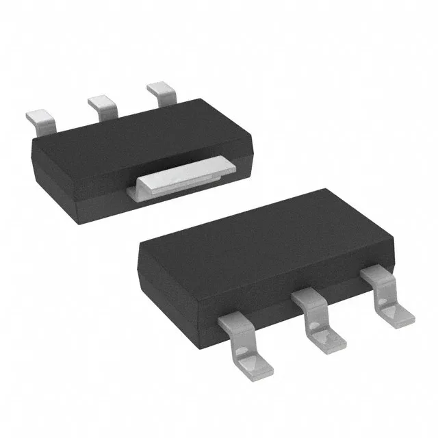
Infineon Technologies BSP295H6327XTSA1

Infineon BSP295H6327XTSA1 N-Channel MOSFET

MPNBSP295H6327XTSA1
End of Life

Infineon SIPMOS® BSP295H6327XTSA1 N-channel MOSFET, 60 V drain-source, 1.8 A continuous drain, 300 mOhm Rds(on) at 10 V, SOT223-4 surface-mount package, -55°C to 150°C junction temperature.

$0.91Ref. price · indicative, final on quote
PackagingTO-261-4, TO-261AA
StockContact for availability
MOQ1 pcs
  • 100% new & originalTraceable channels only — no refurbs, no pulls, no remarked parts.
  • Date & lot codes on quoteStated per line before you commit; label photos on request.
  • MSL-compliant ESD packingMoisture-sealed bags with indicator cards; reels photo-verified.
  • PayPal buyer protectionPay by T/T, PayPal or Payoneer — card payments covered end to end.

Specifications

BSP295H6327XTSA1 Technical Specifications
ParameterValue
SeriesSIPMOS®
FET typeN-Channel
Mounting typeSurface Mount
Drain to source voltage60 V
Drive voltage (Max rds on, min rds on)4.5V, 10V
Current - continuous drain (Id) @ 25°C1.8A (Ta)
Power dissipation1.8W (Ta)
Operating temperature-55°C ~ 150°C (TJ)
PackageTape & Reel (TR); Cut Tape (CT)
Vgs±20V
TechnologyMOSFET (Metal Oxide)
CaseTO-261-4, TO-261AA
Vgs(th) (Max) @ id1.8V @ 400µA
Rds on (Max) @ id, vgs300mOhm @ 1.8A, 10V
Gate charge (Qg) (Max) @ vgs17 nC @ 10 V
Input capacitance (Ciss) (Max) @ vds368 pF @ 25 V

Product details

60 V, 1.8 A N-channel MOSFET in SOT223-4

The Infineon BSP295H6327XTSA1 is a 60 V, 1.8 A N-channel enhancement-mode MOSFET from the SIPMOS® series, housed in a PG-SOT223-4 surface-mount package. It is designed for low-power switching and load-management duties in industrial, automotive, and telecom environments where board space is tight and the junction temperature can reach 150°C. The 300 mOhm maximum on-resistance at 10 V gate drive keeps conduction losses manageable for a device this size; the 1.8 A continuous drain current is the practical load ceiling when the part is soldered to a standard footprint.

Gate drive and switching profile

The gate threshold voltage is 1.8 V maximum at 400 µA drain current. The recommended drive voltage for minimum on-resistance is 10 V, but the part is characterised at both 4.5 V and 10 V. Total gate charge is 17 nC at 10 V, and input capacitance is 368 pF at 25 V drain-source. The ±20 V maximum gate-source rating gives headroom for unregulated gate-drive rails.

Package, mounting, and thermal reality

The PG-SOT223-4 footprint is a four-lead surface-mount package with a large tab for heat transfer to the PCB copper. Maximum power dissipation is 1.8 W at 25°C ambient, derated to zero at 150°C junction. For continuous loads near 1.8 A, a reasonable copper area on the drain tab is required to keep the junction below the thermal limit.

Lifecycle and compliance

The BSP295H6327XTSA1 carries an Active lifecycle status, meaning Infineon continues to manufacture it with no announced last-time-buy or end-of-life. The part is ROHS3 compliant, so it passes the material-restriction requirements for EU and most global markets.

Frequently asked questions

What is the closest functional second-source for BSP295H6327XTSA1?

The IPD50R950CEAUMA1 from Infineon's CoolMOS™ CE series is a 500 V, 4.3 A N-channel MOSFET in a surface-mount package, but its 500 V rating and higher current (4.3 A) target offline power supplies, not the 60 V / 1.8 A low-voltage load-switching role of the BSP295H6327XTSA1. They are not direct functional equivalents — the BSP295H6327XTSA1 is the correct choice for 12 V–48 V auxiliary and load-switch applications.

What package does BSP295H6327XTSA1 come in?

The BSP295H6327XTSA1 is supplied in a PG-SOT223-4 surface-mount package (TO-261-4, TO-261AA equivalent). It is available on Tape & Reel (TR) or Cut Tape (CT) for different assembly volumes.

Is BSP295H6327XTSA1 RoHS compliant?

Yes, the BSP295H6327XTSA1 is ROHS3 compliant, meeting the EU Restriction of Hazardous Substances directive for lead, mercury, cadmium, and other restricted materials.