Depletion-mode N-channel — normally-on switch for fail-safe and linear circuits
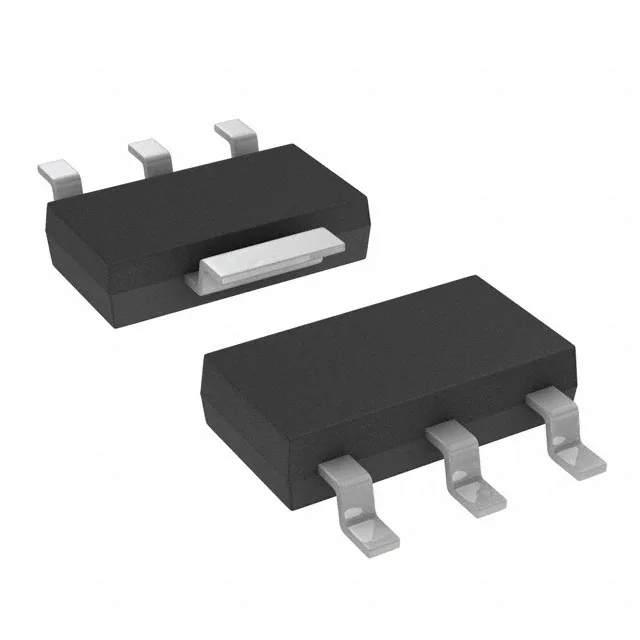
The Infineon BSP149H6327XTSA1 is a SIPMOS® N-channel depletion-mode MOSFET in a PG-SOT223-4 surface-mount package. Unlike the vast majority of enhancement-mode FETs, this device conducts with zero gate-source voltage and requires a negative Vgs to turn off — a normally-on characteristic that suits current-source, linear regulator, and fail-safe bypass applications where a closed switch on gate-drive loss is the desired state. Rated for 200 V drain-source breakdown and 660 mA continuous drain current at 25 °C ambient, with a maximum on-resistance of 1.8 Ohm at 10 V gate drive. The 1.8 W package dissipation limit in the SOT-223 footprint means this part is sized for low-to-moderate power stages, not high-current switching.
The 200 V Vdss sets the maximum off-state drain-to-source voltage. The 660 mA continuous drain current is the package-limited figure at 25 °C. Gate threshold is 1 V maximum at 400 µA drain current, and the part is fully enhanced at 10 V gate drive.
The part is ROHS3 compliant.
Sourcing and fit for production
The depletion-mode behaviour is the key selection criterion — if your circuit requires a normally-on switch, this is the part.