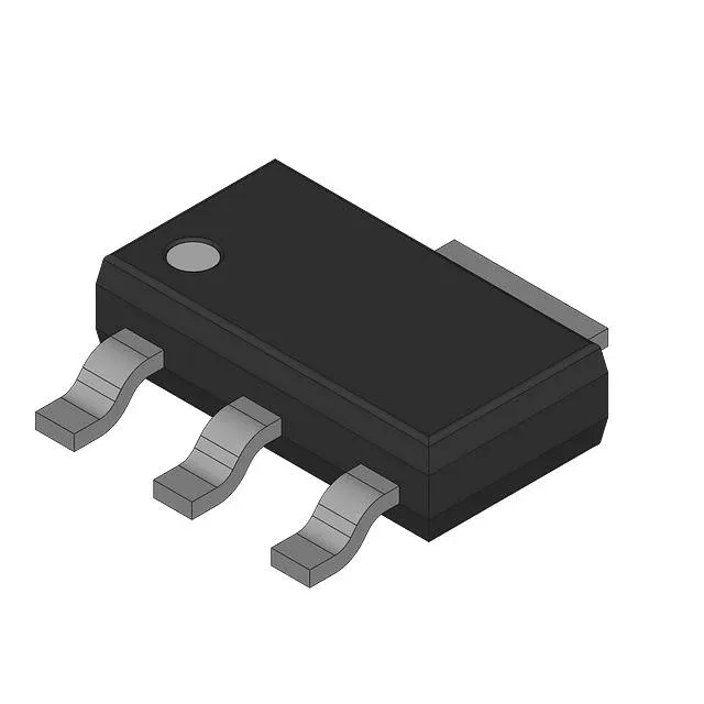
600 V depletion-mode MOSFET in a SOT-223 — what it is for
The depletion-mode characteristic means the channel is normally on at zero gate voltage (Vgs=0V), and a negative gate voltage is required to turn it off — the opposite of an enhancement-mode MOSFET. This makes it the natural choice for normally-on switch applications, current-source circuits, and linear regulators where a depletion-mode device simplifies the control loop.
45 Ohm Rds(on) and 4.9 nC gate charge — switching and conduction trade-offs
That is a high Rds(on) by power MOSFET standards, but the 120 mA current rating keeps conduction losses manageable — at full current the I²R loss is about 0.65 W, within the 1.8 W package dissipation limit. Input capacitance is 146 pF at 25 V Vds, which means the gate-drive rise time is fast even with modest source impedance.
Depletion-mode operation — no negative gate voltage needed for turn-off?
The BSP135L6433 is a depletion-mode MOSFET, so at Vgs=0V the channel conducts. This is a critical design consideration: in a circuit that expects an enhancement-mode part, the BSP135L6433 will conduct continuously unless the gate is actively pulled negative.
PG-SOT223-4-21 package — footprint and thermal reality
The large tab on the package is the drain terminal and provides the primary thermal path. With 1.8 W maximum power dissipation at 25°C ambient, the junction-to-ambient thermal resistance is around 70-80 °C/W depending on PCB copper area. For continuous operation near the 150°C junction limit, a minimum of 1 square inch of copper on the drain tab is recommended.
For new designs, this means no near-term obsolescence risk.