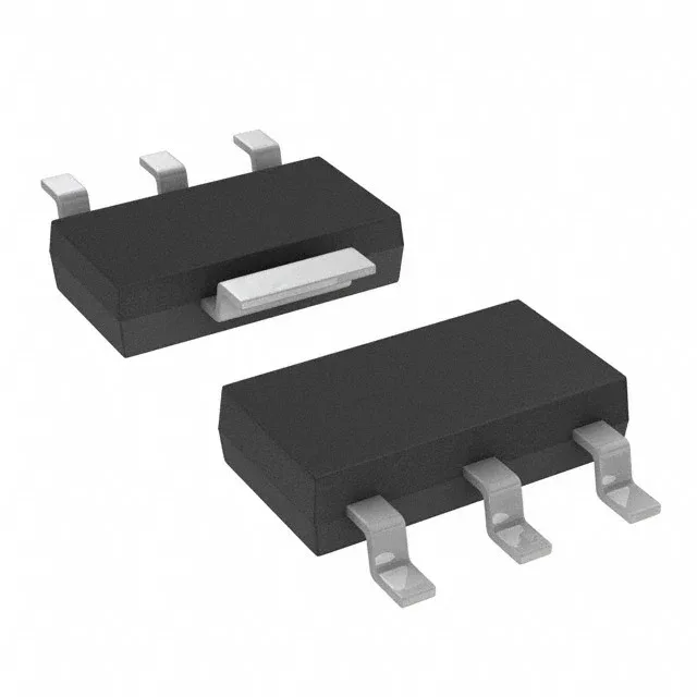
Depletion-mode MOSFET for normally-on and current-source applications
The Infineon BSP129H6327XTSA1 is an N-channel depletion-mode MOSFET from the SIPMOS® series. Unlike a standard enhancement-mode FET, this part conducts at zero gate-source voltage — it is normally on — and requires a negative Vgs to turn it off. That makes it the natural choice for normally-on switch applications, current-limiting circuits, cascode stages, and start-up pass elements where you need conduction at power-up before the gate drive is established. Rated for 240 V drain-source voltage and 350 mA continuous drain current at 25°C, with a maximum on-resistance of 6 Ω at Vgs = 10 V and Id = 350 mA. The low gate charge — 5.7 nC at 5 V — means a simple GPIO or a low-current gate driver can switch it without a dedicated driver IC. Housed in a PG-SOT223-4 surface-mount package, it dissipates up to 1.8 W at 25°C ambient.
The 240 V Vdss is the absolute maximum drain-source voltage the device can block when turned off. It fits DC rails up to 240 V or AC circuits where the peak is clamped below 240 V.
SOT223-4 — rework-friendly footprint
The PG-SOT223-4 package has a large centre tab that is the drain. The 1.8 W dissipation assumes the tab is soldered to a copper pad on the PCB.
It is fully RoHS3 compliant.