P-channel 30V MOSFET in SOIC-8 — what the 21 mΩ Rds(on) means for your load switch
Temperature range and package — where this part fits
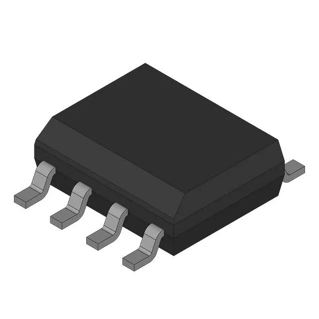
The SOIC-8 footprint (PG-DSO-8-1 supplier package) is a common land pattern, so a board designed for any standard SOIC-8 MOSFET can take this part without a layout change. Power dissipation is limited to 1.56 W at 25°C ambient, so continuous high-current operation needs attention to copper area and airflow — this is not a TO-220 replacement for a 50 W load.
Gate charge and switching — what 54 nC tells the driver designer
That is a moderate figure for a P-channel in an SOIC-8 — a standard gate driver with 1 A peak output can switch it in the tens of nanoseconds. The input capacitance of 2330 pF at 25 V drain is consistent with the gate charge; together they define the driver's peak current requirement and the switching loss at frequency. For a 100 kHz PWM load switch, the gate-drive loss is negligible; at 500 kHz or above, the driver's sourcing capability starts to matter.