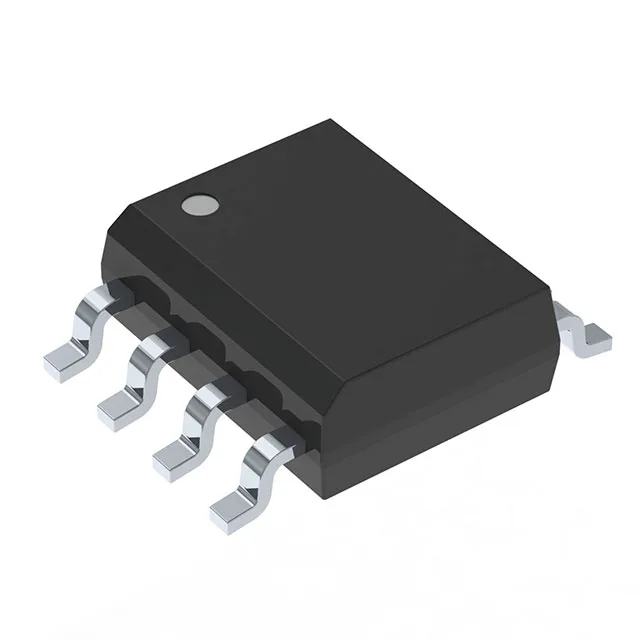
P-channel 30 V MOSFET in SOIC-8 — load-switch and OR-ing duty
The BSO301SPHXUMA1: Housed in the standard 8-pin SOIC package (PG-DSO-8), it is a surface-mount drop-in for existing P-channel designs in this footprint.
The 8 mOhm Rds(on) at Vgs = 10 V is the figure that determines I²R loss in a continuous-duty load switch. At 12.6 A the conduction loss is about 1.27 W — within the 1.79 W maximum power dissipation at 25 °C ambient, but the board copper area and airflow will set the real thermal limit. Gate charge totals 136 nC at 10 V. The 5890 pF input capacitance means the driver output impedance and layout loop inductance matter for clean turn-on edges. For the full 8 mOhm, a 10 V gate rail is required.
Package and thermal reality in the SOIC-8
The PG-DSO-8 package (SOIC-8, 3.90 mm body width) has no exposed pad — all heat dissipates through the leads into the PCB copper. The 1.79 W power dissipation at 25 °C is specified with the device on a standard FR-4 board; for sustained loads near 12.6 A, a 2 oz copper plane and thermal vias under the drain pins are necessary to keep the junction below 150 °C. A 15 V Zener clamp across gate-source is cheap protection if the gate-drive trace is long.