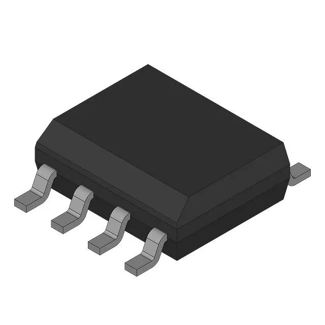
Infineon Technologies BSO203SPNT

Infineon BSO203SPNT P-Channel OptiMOS MOSFET, 20V 9A SOIC-8

MPNBSO203SPNT
End of Life

Infineon OptiMOS® P-Channel Power MOSFET, 20 V drain-source, 9 A continuous drain, 21 mOhm Rds(on) at 4.5 V gate drive, 8-SOIC package, surface mount, -55°C to 150°C junction temperature.

$0.51Ref. price · indicative, final on quote
Packaging8-SOIC (0.154", 3.90mm Width)
StockContact for availability
MOQ1 pcs
  • 100% new & originalTraceable channels only — no refurbs, no pulls, no remarked parts.
  • Date & lot codes on quoteStated per line before you commit; label photos on request.
  • MSL-compliant ESD packingMoisture-sealed bags with indicator cards; reels photo-verified.
  • PayPal buyer protectionPay by T/T, PayPal or Payoneer — card payments covered end to end.

Specifications

BSO203SPNT Technical Specifications
ParameterValue
SeriesOptiMOS®
FET typeP-Channel
Mounting typeSurface Mount
Drain to source voltage20 V
Drive voltage (Max rds on, min rds on)2.5V, 4.5V
Current - continuous drain (Id) @ 25°C9A (Ta)
Power dissipation2.35W (Ta)
Operating temperature-55°C ~ 150°C (TJ)
PackageBulk
Vgs±12V
TechnologyMOSFET (Metal Oxide)
Case8-SOIC (0.154\", 3.90mm Width)
Vgs(th) (Max) @ id1.2V @ 50µA
Rds on (Max) @ id, vgs21mOhm @ 9A, 4.5V
Gate charge (Qg) (Max) @ vgs50.4 nC @ 4.5 V
Input capacitance (Ciss) (Max) @ vds2265 pF @ 15 V

Product details

Package and mounting

The BSO203SPNT: Surface-mount in the PG-DSO-8 (0.154" width, 3.90 mm body) — Infineon's PG-DSO-8 variant. The SOIC-8 footprint is standard, so board layout is straightforward. The thermal pad is the die attach through the package leads; there's no exposed pad, so thermal management relies on the PCB copper area connected to the drain pins. For the 2.35 W dissipation limit, a decent pour on the drain pins is enough for moderate duty cycles, but sustained 9 A will need attention to trace width and via stitching.

Temperature range and environment

Rated for -55°C to 150°C junction temperature — full military-grade temperature span. That makes it suitable for avionics, downhole, or outdoor telecom where the ambient can swing hard. The 150°C Tj max is the silicon limit, but the 2.35 W dissipation at Ta means actual case temperature will be the bottleneck in a hot enclosure.

Lifecycle and sourcing

The part is in current manufacture by Infineon as part of the OptiMOS series. For a BOM line that needs a P-channel SOIC-8 MOSFET at 20 V / 9 A, this is a straightforward fit with no supply chain surprises.

Frequently asked questions

What is the Rds(on) of BSO203SPNT?

The maximum on-resistance is 21 mOhm at 9 A drain current with a 4.5 V gate drive. That's the value to use for conduction loss calculations at the rated current.