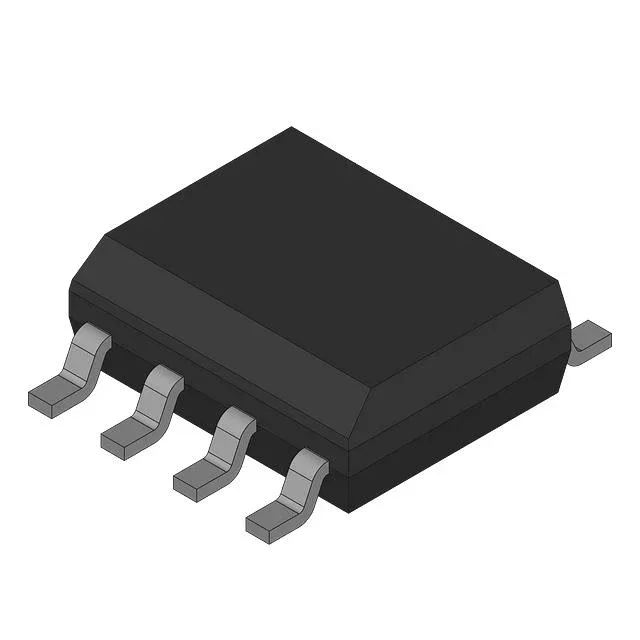
Infineon Technologies BSO203PH — Logic ICs

Infineon BSO203PH OptiMOS Dual P-Channel MOSFET, 20 V, 7 A

MPNBSO203PH
End of Life

Infineon OptiMOS® BSO203PH, dual P-Channel MOSFET, 20 V Vdss, 7 A continuous drain, 21 mOhm Rds(on) max at 4.5 V gate drive, logic-level gate, 1.6 W power dissipation, surface-mount PG-DSO-8 package.

$0.61Ref. price · indicative, final on quote
Packaging8-SOIC (0.154", 3.90mm Width)
StockContact for availability
MOQ1 pcs
  • 100% new & originalTraceable channels only — no refurbs, no pulls, no remarked parts.
  • Date & lot codes on quoteStated per line before you commit; label photos on request.
  • MSL-compliant ESD packingMoisture-sealed bags with indicator cards; reels photo-verified.
  • PayPal buyer protectionPay by T/T, PayPal or Payoneer — card payments covered end to end.

Specifications

BSO203PH Technical Specifications
ParameterValue
SeriesOptiMOS®
FET type2 P-Channel (Dual)
Mounting typeSurface Mount
Drain to source voltage20V
Current - continuous drain (Id) @ 25°C7A (Ta)
Power - max1.6W (Ta)
Operating temperature-55°C ~ 150°C (TJ)
PackageBulk
FET featureLogic Level Gate
Case8-SOIC (0.154\", 3.90mm Width)
Vgs(th) (Max) @ id1.2V @ 50µA
Rds on (Max) @ id, vgs21mOhm @ 8.2A, 4.5V
Gate charge (Qg) (Max) @ vgs39nC @ 4.5V
Input capacitance (Ciss) (Max) @ vds3750pF @ 15V

Product details

The Infineon BSO203PH is a dual P-channel enhancement-mode MOSFET from the OptiMOS® family, built for low-voltage power switching where two matched P-FETs are needed in a single SOIC-8 footprint. The 1.6 W package-level power limit means the thermal budget is tight for continuous high-current operation; this part is sized for load-switching, battery-protection, or power-rail OR-ing where the average dissipation stays low and the SOIC-8 copper footprint can sink the heat.

21 mOhm at 4.5 V — what the on-resistance means for your BOM

The 21 mOhm Rds(on) is specified at 4.5 V gate drive, not the usual 10 V. At 7 A the conduction loss is roughly 1 W per channel (I² × R), which eats into the 1.6 W package limit — derate for ambient temperature above 25 °C. If your load is intermittent or you parallel the two channels, the effective resistance drops to about 10.5 mOhm, splitting the dissipation across both dice.

Package and thermal handling for the layout

The part ships in an 8-pin SOIC package (PG-DSO-8, 3.90 mm body width). The two P-channel dice share the same substrate; the exposed pad on the bottom of the package is the common drain connection. For the 1.6 W max dissipation to be usable, the PCB copper area under the package must be stitched with vias to an inner-layer ground plane — without that thermal path the junction temperature rises quickly above 150 °C at continuous current. The gate charge is 39 nC at 4.5 V, so the switching losses at moderate frequency (100–200 kHz) are manageable from a standard MCU GPIO.

Frequently asked questions

What is the closest pin-compatible alternative to BSO203PH?

Within the same OptiMOS family, Infineon offers several dual P-channel parts in the PG-DSO-8 footprint, but the exact Rds(on) and current rating vary by variant.