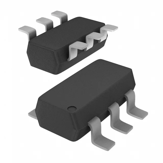
Infineon Technologies BSL215CH6327XTSA1

BSL215CH6327XTSA1 OptiMOS™ MOSFET, N/P-CH 20V 1.5A, AEC-Q101

MPNBSL215CH6327XTSA1
End of Life

Infineon OptiMOS™ BSL215CH6327XTSA1, Automotive Grade N and P-Channel Complementary MOSFET, 20V Vdss, 1.5A Id, 140mOhm Rds(on) @ 1.5A 4.5V, Logic Level Gate 2.5V Drive, PG-TSOP6-6 package, AEC-Q101 qualified.

$0.63Ref. price · indicative, final on quote
PackagingSOT-23-6 Thin, TSOT-23-6
StockContact for availability
MOQ1 pcs
  • 100% new & originalTraceable channels only — no refurbs, no pulls, no remarked parts.
  • Date & lot codes on quoteStated per line before you commit; label photos on request.
  • MSL-compliant ESD packingMoisture-sealed bags with indicator cards; reels photo-verified.
  • PayPal buyer protectionPay by T/T, PayPal or Payoneer — card payments covered end to end.

Specifications

BSL215CH6327XTSA1 Technical Specifications
ParameterValue
SeriesOptiMOS™
Mounting typeSurface Mount
Drain to source voltage20V
Current - continuous drain (Id) @ 25°C1.5A
Power - max500mW
Operating temperature-55°C ~ 150°C (TJ)
GradeAutomotive
PackageTape & Reel (TR); Cut Tape (CT)
TechnologyMOSFET (Metal Oxide)
FET featureLogic Level Gate, 2.5V Drive
ConfigurationN and P-Channel Complementary
QualificationAEC-Q101
CaseSOT-23-6 Thin, TSOT-23-6
Vgs(th) (Max) @ id1.2V @ 3.7µA
Rds on (Max) @ id, vgs140mOhm @ 1.5A, 4.5V
Gate charge (Qg) (Max) @ vgs0.73nC @ 4.5V
Input capacitance (Ciss) (Max) @ vds143pF @ 10V

Product details

Complementary N/P-channel pair in a single TSOP6-6

The Infineon BSL215CH6327XTSA1 is an OptiMOS™ series complementary MOSFET that integrates one N-channel and one P-channel device in a single PG-TSOP6-6 surface-mount package. Rated for 20 V drain-source voltage and 1.5 A continuous drain current per channel, it is qualified to AEC-Q101 and specified across a -55 °C to 150 °C junction temperature range. Each channel is a logic-level gate device specified for 2.5 V drive. Maximum on-resistance is 140 mOhm at 1.5 A with a 4.5 V gate drive; gate charge is 0.73 nC at 4.5 V.

Package and footprint

The part comes in a PG-TSOP6-6 package, a thin SOT-23-6 variant with 6 leads. It is supplied on Tape & Reel or Cut Tape, suited for automated pick-and-place assembly. The complementary pair in one package saves board area compared to two separate SOT-23 devices, and the TSOP profile suits height-constrained enclosures.

Design considerations for the complementary pair

Total power dissipation is limited to 500 mW across the package. Maximum input capacitance is 143 pF at 10 V drain-source.

Lifecycle and sourcing position

The BSL215CH6327XTSA1 carries an active lifecycle status with ROHS3 compliance.

Frequently asked questions

Is BSL215CH6327XTSA1 automotive qualified?

Yes, the BSL215CH6327XTSA1 is qualified to AEC-Q101, the automotive stress test qualification for discrete semiconductors. It is also rated Automotive Grade and specified for a junction temperature range of -55 °C to 150 °C.