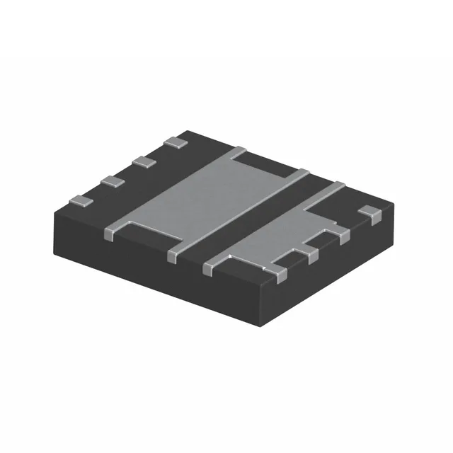
Infineon Technologies BSG0811NDATMA1

Infineon BSG0811NDATMA1 OptiMOS Dual N-Ch MOSFET

MPNBSG0811NDATMA1
End of Life

Infineon OptiMOS BSG0811NDATMA1, dual N-channel asymmetrical MOSFET, 25V Vdss, 3mOhm Rds(on) at 10V, 19A/41A continuous drain, logic-level gate, PG-TISON-8 surface mount, -55 to 150°C.

$3.26Ref. price · indicative, final on quote
Packaging8-PowerTDFN
StockContact for availability
MOQ1 pcs
  • 100% new & originalTraceable channels only — no refurbs, no pulls, no remarked parts.
  • Date & lot codes on quoteStated per line before you commit; label photos on request.
  • MSL-compliant ESD packingMoisture-sealed bags with indicator cards; reels photo-verified.
  • PayPal buyer protectionPay by T/T, PayPal or Payoneer — card payments covered end to end.

Specifications

BSG0811NDATMA1 Technical Specifications
ParameterValue
SeriesOptiMOS™
Mounting typeSurface Mount
Drain to source voltage25V
Current - continuous drain (Id) @ 25°C19A, 41A
Power - max2.5W
Operating temperature-55°C ~ 150°C (TJ)
PackageTape & Reel (TR); Cut Tape (CT)
TechnologyMOSFET (Metal Oxide)
FET featureLogic Level Gate, 4.5V Drive
Configuration2 N-Channel (Dual) Asymmetrical
Case8-PowerTDFN
Vgs(th) (Max) @ id2V @ 250µA
Rds on (Max) @ id, vgs3mOhm @ 20A, 10V
Gate charge (Qg) (Max) @ vgs8.4nC @ 4.5V
Input capacitance (Ciss) (Max) @ vds1100pF @ 12V

Product details

What this OptiMOS dual FET is and where it fits

The Infineon BSG0811NDATMA1 is a dual N-channel asymmetrical power MOSFET from the OptiMOS series, rated for 25V drain-to-source and delivering 19A continuous on one channel and 41A on the other. Packaged in a PG-TISON-8, it targets space-constrained power stages where two FETs share a common drain pad and the load currents are unequal — typical in synchronous buck converters, motor driver half-bridges, and battery management switching paths.

Asymmetric channels — why the different current ratings

One channel is rated for 19A continuous, the other for 41A. This asymmetry matches a half-bridge where the low-side FET carries the inductor current for a larger portion of the switching period (synchronous buck) or where the high-side sees pulsed current while the low-side handles the DC freewheel current. The 2.5W package power limit means the total dissipation across both channels combined is the real constraint in a real board — the 41A figure assumes ideal heatsinking on the larger channel.

Temperature range and environment

Junction temperature spans -55°C to 150°C, covering automotive under-hood and industrial motor-drive environments. The PG-TISON-8 package is a surface-mount power package with an exposed pad for thermal transfer to the PCB copper plane — plan a thermal via array under the part to keep junction temperature within limits at the 19A or 41A continuous currents.

Lifecycle and sourcing

No end-of-life notice on record, so this part is safe to specify into new designs without an LTB risk.

Frequently asked questions

Can BSG0811NDATMA1 be used in a motor driver circuit?

Yes. The dual asymmetrical N-channel configuration with one channel rated for 19A and the other for 41A at 25V Vdss is suited for a motor driver half-bridge. The logic-level gate drive allows direct connection to a 3.3V or 5V MCU PWM output. The 3mOhm Rds(on) keeps conduction losses low, but the 2.5W package power limit means the total dissipation across both channels must be managed with adequate PCB heatsinking.

What is the closest pin-compatible alternative to BSG0811NDATMA1 in this component family?

The BSG0810ND is a known sibling in the same OptiMOS family and same PG-TISON-8 package. Verify the pinout and electrical ratings against your design before substituting — the BSG0811NDATMA1 has asymmetric 19A/41A channels, while the BSG0810ND may carry different current ratings or Rds(on) values.