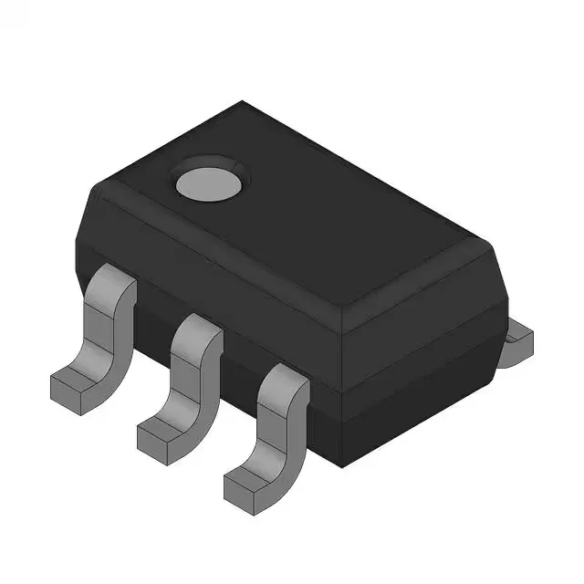
Infineon Technologies BSD314SPE L6327 — Discrete Semiconductors

Infineon BSD314SPE L6327 P-Channel MOSFET, 30 V, 1.5 A

MPNBSD314SPE L6327
Active

Infineon OptiMOS™-P 3 P-Channel MOSFET, 30 V drain-source, 1.5 A continuous drain current, 140 mOhm on-resistance at 10 V gate drive, ±20 V gate-source rating, -55°C to 150°C junction temperature, surface-mount Bulk package.

$0.05Ref. price · indicative, final on quote
StockContact for availability
MOQ1 pcs
  • 100% new & originalTraceable channels only — no refurbs, no pulls, no remarked parts.
  • Date & lot codes on quoteStated per line before you commit; label photos on request.
  • MSL-compliant ESD packingMoisture-sealed bags with indicator cards; reels photo-verified.
  • PayPal buyer protectionPay by T/T, PayPal or Payoneer — card payments covered end to end.

Specifications

BSD314SPE L6327 Technical Specifications
ParameterValue
SeriesOptiMOS™-P 3
FET typeP-Channel
Mounting_typeSurface Mount
Operating temperature high-55°C to 150°C(TJ)
Vgs±20 V
Power_w0.5
Package_typeBulk
Capacitance_uf0.0003
Product_statusActive
Supply_voltage_v30.0
Vgs(Th) (Max) @ id2 V @ 6.3µA
Switching_current_a1.5
Rds on (Max) @ id, vgs140mOhm @ 1.5 A, 10 V
Gate charge (Qg) (Max) @ vgs2.9 nC @ 10 V

Product details

P-Channel switch for 30 V rails — what the ratings tell you

The Infineon BSD314SPE L6327 is a P-Channel enhancement-mode MOSFET from the OptiMOS™-P 3 family, rated for a 30 V drain-source voltage and 1.5 A continuous drain current. The ±20 V gate-source rating gives headroom for gate-drive transients, but the 2 V typical threshold (at 6.3 µA) means the device is fully enhanced well below 10 V — useful for 5 V or 3.3 V gate-drive designs where Rds(on) will be higher than the 10 V figure. This makes the part a candidate for engine-bay electronics, outdoor telecom cabinets, or any environment where ambient temperature exceeds 85°C and the thermal design must budget for self-heating.

Switching loss and gate-drive budget

Total gate charge at 10 V is 2.9 nC. At a 500 kHz switching frequency, the average gate-drive current needed is about 1.45 mA — easily supplied by a standard MOSFET driver or a microcontroller GPIO with a series resistor. The low Qg keeps switching losses small in high-frequency DC-DC converters and load switches. The 0.5 W power dissipation rating sets the thermal limit for continuous operation. With Rds(on) at 140 mOhm, the maximum continuous current at 25°C ambient (assuming no heatsink) is roughly 1.9 A before hitting the 0.5 W ceiling — so the 1.5 A rated current is already thermally limited in free air. In a real board with copper pour and airflow, the usable current may be higher, but the 0.5 W figure is the absolute thermal budget for the die.

Package and supply chain note

The part is — loose devices in a bag or tube, not Tape & Reel. For automated pick-and-place, you will need to transfer to a feeder-compatible carrier. The surface-mount package is suitable for reflow soldering; the lead-free finish is compatible with standard Pb-free profiles.

Frequently asked questions

What is the maximum Vgs for BSD314SPE L6327?

The maximum gate-source voltage is ±20 V. Exceeding this rating can damage the gate oxide. The 2 V typical threshold means the device turns on well below 10 V, but the Rds(on) is specified at 10 V gate drive.