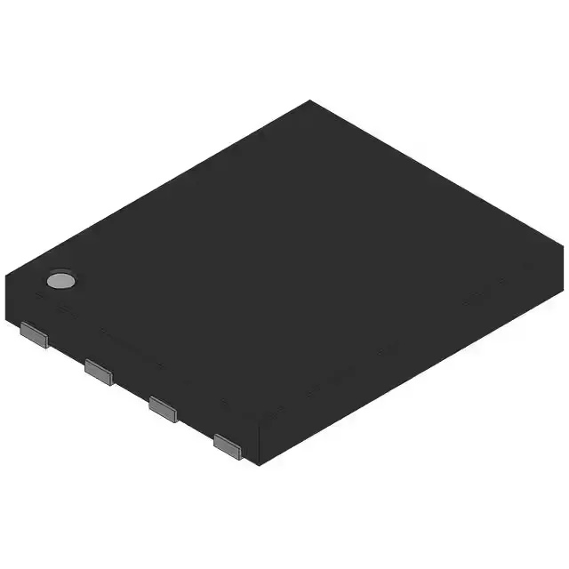
Infineon Technologies BSC8899N03MS

Infineon BSC8899N03MS N-Channel MOSFET, 30 V, 9 mOhm

MPNBSC8899N03MS
End of Life

Infineon OptiMOS® 3 N-Channel MOSFET, BSC8899N03MS, 30 V Vdss, 9 mOhm Rds(on) at 30 A, 10 V, 16 nC gate charge, PG-TDSON-8-6 package, -55 to 150 °C.

$0.27Ref. price · indicative, final on quote
Packaging8-PowerTDFN
StockContact for availability
MOQ1 pcs
  • 100% new & originalTraceable channels only — no refurbs, no pulls, no remarked parts.
  • Date & lot codes on quoteStated per line before you commit; label photos on request.
  • MSL-compliant ESD packingMoisture-sealed bags with indicator cards; reels photo-verified.
  • PayPal buyer protectionPay by T/T, PayPal or Payoneer — card payments covered end to end.

Specifications

BSC8899N03MS Technical Specifications
ParameterValue
SeriesOptiMOS® 3
FET typeN-Channel
Mounting typeSurface Mount
Drain to source voltage30 V
Drive voltage (Max rds on, min rds on)4.5V, 10V
Current - continuous drain (Id) @ 25°C13A (Ta), 45A (Tc)
Power dissipation2.5W (Ta), 28W (Tc)
Operating temperature-55°C ~ 150°C (TJ)
PackageBulk
Vgs±20V
TechnologyMOSFET (Metal Oxide)
Case8-PowerTDFN
Vgs(th) (Max) @ id2.2V @ 250µA
Rds on (Max) @ id, vgs9mOhm @ 30A, 10V
Gate charge (Qg) (Max) @ vgs16 nC @ 10 V
Input capacitance (Ciss) (Max) @ vds1300 pF @ 15 V

Product details

What this 30 V N-channel MOSFET is for

The Infineon BSC8899N03MS is an N-channel power MOSFET from the OptiMOS® 3 family, built for low-voltage DC-DC conversion, load switching, and motor-drive applications. It handles a continuous drain current of 13 A at the board level (Ta) and 45 A when the case is properly heatsunk (Tc), so the real-world limit depends on your PCB copper and airflow. The 9 mOhm on-resistance at 30 A and 10 V gate drive keeps conduction losses low enough that a 2.5 W board-level dissipation budget is realistic — but that 28 W case-rated maximum tells you the package can deliver if you pull the heat out through the PG-TDSON-8-6 footprint.

Gate drive and switching

The 16 nC gate charge at 10 V is moderate for a 30 V part in this current class.

Temperature range and environment

The -55°C to 150°C junction temperature range covers military and industrial extremes.

Package and footprint

The PG-TDSON-8-6 (8-PowerTDFN) is a surface-mount package with an exposed drain pad on the bottom. That pad is the main thermal path — you need a copper plane and vias under it to get the 28 W case-rated dissipation. The footprint is hand-solderable with a hot-air station if you're prototyping, but for production, reflow with a proper solder-paste stencil is the way to go. The ±20 V maximum gate-source voltage gives you margin against gate spikes in half-bridge configurations.

Frequently asked questions

What package is BSC8899N03MS?

It comes in a PG-TDSON-8-6 package, which is an 8-lead PowerTDFN with an exposed drain pad for thermal management.

What is the lead time for BSC8899N03MS?

Lead time is confirmed at quote time through our sourcing desk. Submit an RFQ for the current lead-time estimate — it varies with factory load and order quantity.