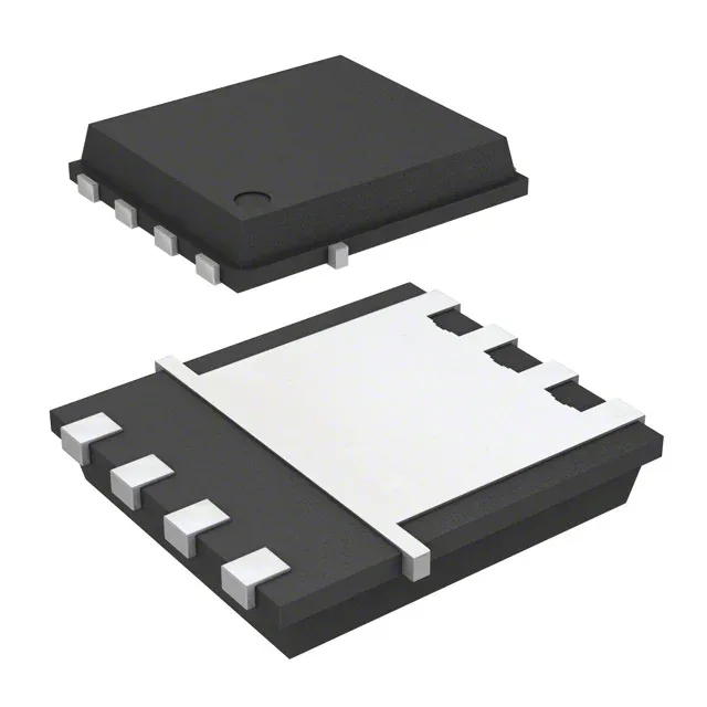
Infineon Technologies BSC500N20NS3GATMA1

Infineon BSC500N20NS3GATMA1 N-Channel MOSFET, 200V 24A

MPNBSC500N20NS3GATMA1
End of Life

Infineon OptiMOS™ BSC500N20NS3GATMA1, N-Channel MOSFET, 200 V Vdss, 24 A continuous drain, 50 mOhm Rds(on) at 10 V, 15 nC gate charge, PG-TDSON-8-1 package, -55°C to 150°C junction temperature.

$2.15Ref. price · indicative, final on quote
Packaging8-PowerTDFN
StockContact for availability
MOQ1 pcs
  • 100% new & originalTraceable channels only — no refurbs, no pulls, no remarked parts.
  • Date & lot codes on quoteStated per line before you commit; label photos on request.
  • MSL-compliant ESD packingMoisture-sealed bags with indicator cards; reels photo-verified.
  • PayPal buyer protectionPay by T/T, PayPal or Payoneer — card payments covered end to end.

Specifications

BSC500N20NS3GATMA1 Technical Specifications
ParameterValue
SeriesOptiMOS™
FET typeN-Channel
Mounting typeSurface Mount
Drain to source voltage200 V
Drive voltage (Max rds on, min rds on)10V
Current - continuous drain (Id) @ 25°C24A (Tc)
Power dissipation96W (Tc)
Operating temperature-55°C ~ 150°C (TJ)
PackageTape & Reel (TR); Cut Tape (CT)
Vgs±20V
TechnologyMOSFET (Metal Oxide)
Case8-PowerTDFN
Vgs(th) (Max) @ id4V @ 60µA
Rds on (Max) @ id, vgs50mOhm @ 22A, 10V
Gate charge (Qg) (Max) @ vgs15 nC @ 10 V
Input capacitance (Ciss) (Max) @ vds1580 pF @ 100 V

Product details

Rds(on) and gate charge — what they mean for the switching stage

The 50 mOhm maximum on-resistance at 22 A and 10 V gate drive is the figure that determines conduction loss in the on-state. At that current level, the I²R loss is roughly 24 W, which the 96 W package power dissipation can handle with adequate heatsinking. The 15 nC gate charge at 10 V is low enough that a standard 1 A gate-driver IC can switch the MOSFET in the tens-of-nanoseconds range, keeping crossover losses in check for a 200 V rail. This combination — moderate Rds(on) with low gate charge — makes the part a good fit for a 200 V input half-bridge or a flyback primary switch where board space is tight and the TDSON-8 package saves area over a DPAK or D2PAK.

Active lifecycle and ROHS3 compliance

Active product status from Infineon, ROHS3 compliant.

Frequently asked questions

Is BSC500N20NS3GATMA1 RoHS compliant?

Yes, the BSC500N20NS3GATMA1 is ROHS3 compliant, meeting the latest EU restriction-of-hazardous-substances directive.

What is the closest functional second-source for BSC500N20NS3GATMA1?

The IPD50R950CEAUMA1 is a different device class — a 500 V CoolMOS™ CE with 950 mOhm Rds(on) and 4.3 A drain current. It is not a pin-compatible or functional second-source for the 200 V, 24 A BSC500N20NS3GATMA1. For a 200 V N-channel MOSFET in a small footprint, stay within the OptiMOS™ 200 V family.