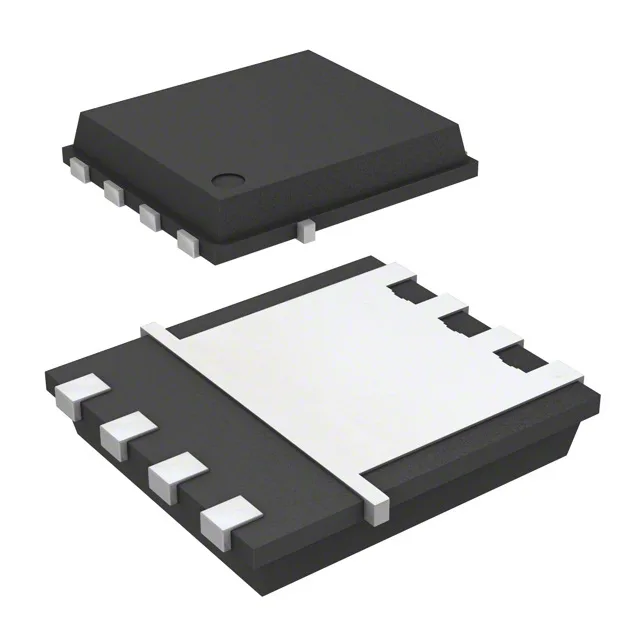
The Infineon BSC190N12NS3GATMA1 is a 120 V N-channel MOSFET from the OptiMOS series, built for medium-voltage switching where conduction loss matters. The 19 mOhm typical on-resistance at 10 V gate drive keeps dissipation low in a 44 A continuous-drain design at case temperature, though the 8.6 A rating at ambient is the real limit on a bare board without a heatsink. The 8-PowerTDFN package (PG-TDSON-8-1) is a surface-mount, thermally enhanced footprint that pulls heat into the PCB copper — expect to pour copper on the drain tab if you plan to push past a few amps.
Gate drive and switching — 10 V is the target
This part is specified for a 10 V gate drive to achieve minimum Rds(on); the gate threshold is 4 V max at 42 µA drain current, but don't expect full enhancement below 10 V. The ±20 V Vgs max gives headroom for ringing on long gate traces, but keep the steady-state drive at 10 V to stay inside the safe operating area.
Temperature range and thermal limits
If the board runs hot, derate the continuous current from the 44 A Tc figure; the 8.6 A Ta rating is the conservative starting point for a convection-cooled layout.
ROHS3 compliance is confirmed, which simplifies compliance for EU and RoHS-regulated markets.