100 V, 63 A N-channel in PG-TDSON-8-1 — the switching-loss and thermal budget
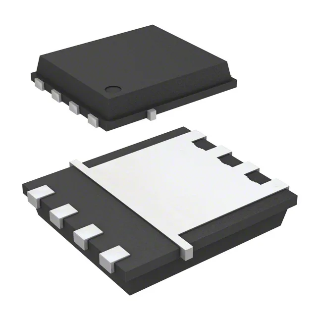
The BSC109N10NS3GATMA1: The part lives in an 8-PowerTDFN (PG-TDSON-8-1) surface-mount package with an exposed drain pad for thermal transfer to the board. The junction temperature range of -55 to 150 °C covers automotive under-hood and industrial environments.
That is the worst-case resistance a designer uses for I²R loss calculations at full load.
Gate charge and input capacitance — driver and switching-loss reality
No last-time-buy notice or end-of-life signal is present.
Mounting and thermal — the exposed pad matters
The PG-TDSON-8-1 package is an 8-lead PowerTDFN with a large exposed drain pad on the bottom.