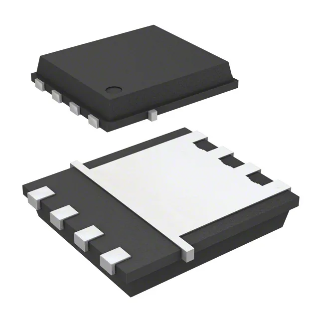
Infineon Technologies BSC100N10NSFGATMA1

Infineon BSC100N10NSFGATMA1 N-Channel MOSFET, 100V, 90A

MPNBSC100N10NSFGATMA1
End of Life

Infineon OptiMOS™ N-Channel MOSFET, 100 V drain-source, 11.4 A (Ta) / 90 A (Tc) continuous drain, 10 mOhm Rds(on) at 10 V, 8-PowerTDFN (PG-TDSON-8-1) package, -55°C to 150°C junction temperature.

$2.3Ref. price · indicative, final on quote
Packaging8-PowerTDFN
StockContact for availability
MOQ1 pcs
  • 100% new & originalTraceable channels only — no refurbs, no pulls, no remarked parts.
  • Date & lot codes on quoteStated per line before you commit; label photos on request.
  • MSL-compliant ESD packingMoisture-sealed bags with indicator cards; reels photo-verified.
  • PayPal buyer protectionPay by T/T, PayPal or Payoneer — card payments covered end to end.

Specifications

BSC100N10NSFGATMA1 Technical Specifications
ParameterValue
SeriesOptiMOS™
FET typeN-Channel
Mounting typeSurface Mount
Drain to source voltage100 V
Drive voltage (Max rds on, min rds on)10V
Current - continuous drain (Id) @ 25°C11.4A (Ta), 90A (Tc)
Power dissipation156W (Tc)
Operating temperature-55°C ~ 150°C (TJ)
PackageTape & Reel (TR); Cut Tape (CT)
Vgs±20V
TechnologyMOSFET (Metal Oxide)
Case8-PowerTDFN
Vgs(th) (Max) @ id4V @ 110µA
Rds on (Max) @ id, vgs10mOhm @ 25A, 10V
Gate charge (Qg) (Max) @ vgs44 nC @ 10 V
Input capacitance (Ciss) (Max) @ vds2900 pF @ 50 V

Product details

100 V, 90 A N-channel MOSFET in a compact TDSON-8 package

The Infineon BSC100N10NSFGATMA1 is an N-channel enhancement-mode MOSFET from the OptiMOS™ family, rated for 100 V drain-source voltage and 90 A continuous drain current at case temperature. The 10 mOhm maximum on-resistance at 10 V gate drive keeps conduction losses low in high-current paths such as synchronous rectification, motor-drive output stages, and DC-DC converters. The 8-PowerTDFN package (PG-TDSON-8-1) provides a compact footprint with an exposed pad for thermal transfer to the PCB.

Gate drive and switching characteristics

The device requires a 10 V gate drive to achieve the rated Rds(on); the gate threshold voltage is 4 V maximum at 110 µA drain current. Gate charge is 44 nC at 10 V, and input capacitance is 2900 pF at 50 V drain-source. These figures define the gate-driver current and switching loss budget — a 10 V gate-drive supply is assumed, and the driver must source and sink the 44 nC per cycle at the intended switching frequency.

Thermal and environmental ratings

Junction temperature range spans -55°C to 150°C, covering automotive under-hood and industrial enclosure environments. Maximum power dissipation is 156 W at case temperature. The part is ROHS3 compliant and carries an active lifecycle status — no end-of-life notice, no last-time-buy window to manage.

Frequently asked questions

Is BSC100N10NSFGATMA1 RoHS compliant?

Yes, the part is ROHS3 compliant per the manufacturer's specification.

What is the lead time for BSC100N10NSFGATMA1?

Lead time is confirmed at quote time against an RFQ. As an active part with broad distribution, typical lead times are manageable, but the exact figure depends on current factory backlog and distributor inventory — request a quote for the current lead-time estimate.