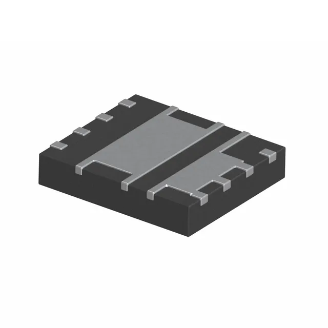
Infineon Technologies BSC0911NDATMA1

BSC0911NDATMA1 OptiMOS™ Dual N-Ch MOSFET, 25V 18A/30A

MPNBSC0911NDATMA1
End of Life

Infineon OptiMOS™ BSC0911NDATMA1, dual N-channel asymmetrical MOSFET, 25V Vdss, 18A/30A continuous drain, 3.2mOhm Rds(on), logic-level gate, PG-TISON-8 package, -55 to 150°C junction temperature.

$1.83Ref. price · indicative, final on quote
Packaging8-PowerTDFN
StockContact for availability
MOQ1 pcs
  • 100% new & originalTraceable channels only — no refurbs, no pulls, no remarked parts.
  • Date & lot codes on quoteStated per line before you commit; label photos on request.
  • MSL-compliant ESD packingMoisture-sealed bags with indicator cards; reels photo-verified.
  • PayPal buyer protectionPay by T/T, PayPal or Payoneer — card payments covered end to end.

Specifications

BSC0911NDATMA1 Technical Specifications
ParameterValue
SeriesOptiMOS™
Mounting typeSurface Mount
Drain to source voltage25V
Current - continuous drain (Id) @ 25°C18A, 30A
Power - max1W
Operating temperature-55°C ~ 150°C (TJ)
PackageTape & Reel (TR); Cut Tape (CT)
TechnologyMOSFET (Metal Oxide)
FET featureLogic Level Gate, 4.5V Drive
Configuration2 N-Channel (Dual) Asymmetrical
Case8-PowerTDFN
Vgs(th) (Max) @ id2V @ 250µA
Rds on (Max) @ id, vgs3.2mOhm @ 20A, 10V
Gate charge (Qg) (Max) @ vgs12nC @ 4.5V
Input capacitance (Ciss) (Max) @ vds1600pF @ 12V

Product details

Dual asymmetrical MOSFET in a TISON-8 — what the ratings mean for your load switch

The Infineon BSC0911NDATMA1 is a dual N-channel asymmetrical MOSFET from the OptiMOS™ series, housed in a PG-TISON-8 surface-mount package. It integrates two separate FETs on one die: one rated for 18A continuous drain, the other for 30A, both with a 25V drain-to-source breakdown. The asymmetry lets you size the high-side and low-side independently in a synchronous buck or use the higher-rated channel for the main pass and the lower-rated for an OR-ing or load-switch leg — no need to over-spec both halves. The junction temperature range of -55°C to 150°C covers automotive under-hood and industrial outdoor enclosures without derating. Input capacitance is 1600pF at 12V Vds — moderate for a dual 25V part, so the gate driver doesn't need a high peak-current buffer for moderate switching frequencies.

Lifecycle and compliance — no LTB risk, ROHS3 documented

The BSC0911NDATMA1 carries an Active lifecycle status. No PCN-driven BOM freeze is required for this line item today.

Package and mounting — PG-TISON-8 footprint

The supplier device package is PG-TISON-8, a power quad flat no-lead with an exposed pad for thermal dissipation. The 8-PowerTDFN case code is the industry-standard footprint; the exposed pad must be soldered to a copper plane on the PCB to achieve the rated 1W maximum power dissipation. Tape & Reel and Cut Tape options are listed for the shipping medium, so the part fits standard pick-and-place lines.

Frequently asked questions

What is the closest pin-compatible alternative to the BSC0911NDATMA1?

No pin-compatible second source is listed in the available documentation. The part is an Infineon proprietary OptiMOS™ design; for a dual-sourcing strategy, evaluate other dual N-channel MOSFETs in the same PG-TISON-8 footprint with similar 25V Vdss and logic-level gate drive, but verify pinout and thermal pad compatibility against the datasheet.