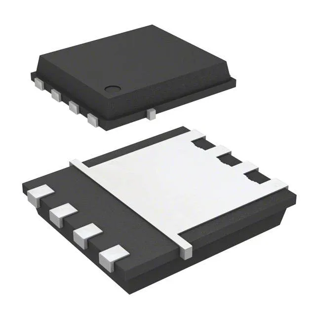
Infineon Technologies BSC090N03LSGATMA1

BSC090N03LSGATMA1 Infineon OptiMOS N-Ch 30V MOSFET

MPNBSC090N03LSGATMA1
End of Life

Infineon OptiMOS™ N-Channel MOSFET, 30 V drain-source, 9 mOhm Rds(on) max at 10 V gate drive, 48 A continuous drain at case temp, 18 nC gate charge, PG-TDSON-8-5 package, -55°C to 150°C junction temperature.

$0.68Ref. price · indicative, final on quote
Packaging8-PowerTDFN
StockContact for availability
MOQ1 pcs
  • 100% new & originalTraceable channels only — no refurbs, no pulls, no remarked parts.
  • Date & lot codes on quoteStated per line before you commit; label photos on request.
  • MSL-compliant ESD packingMoisture-sealed bags with indicator cards; reels photo-verified.
  • PayPal buyer protectionPay by T/T, PayPal or Payoneer — card payments covered end to end.

Specifications

BSC090N03LSGATMA1 Technical Specifications
ParameterValue
SeriesOptiMOS™
FET typeN-Channel
Mounting typeSurface Mount
Drain to source voltage30 V
Drive voltage (Max rds on, min rds on)4.5V, 10V
Current - continuous drain (Id) @ 25°C13A (Ta), 48A (Tc)
Power dissipation2.5W (Ta), 32W (Tc)
Operating temperature-55°C ~ 150°C (TJ)
PackageTape & Reel (TR); Cut Tape (CT)
Vgs±20V
TechnologyMOSFET (Metal Oxide)
Case8-PowerTDFN
Vgs(th) (Max) @ id2.2V @ 250µA
Rds on (Max) @ id, vgs9mOhm @ 30A, 10V
Gate charge (Qg) (Max) @ vgs18 nC @ 10 V
Input capacitance (Ciss) (Max) @ vds1500 pF @ 15 V

Product details

OptiMOS 30 V N-channel — what the ratings mean for the board

The Infineon BSC090N03LSGATMA1 is an N-channel enhancement-mode MOSFET from the OptiMOS™ family, rated for 30 V drain-source breakdown and packaged in a PG-TDSON-8-5 (8-PowerTDFN) surface-mount footprint. It targets low-voltage DC-DC converters, load switches, and battery protection circuits where conduction loss and board area are the primary constraints. The headline on-resistance is 9 mOhm maximum at 10 V gate drive with 30 A drain current — that is the figure that sets the I²R loss in a synchronous rectifier or high-current OR-ing diode replacement. At 48 A continuous drain current (Tc), the silicon itself can carry the load, but the 2.5 W at ambient vs 32 W at case tells you the board copper and any heatsink define the real thermal limit. Gate charge of 18 nC at 10 V is specified. The ±20 V maximum gate-source rating and 4.5 V, 10 V drive voltage are listed. Junction temperature range of -55°C to 150°C covers automotive under-hood and industrial motor-drive environments where the PCB sees sustained heat soak. Input capacitance of 1500 pF at 15 V Vds is moderate — the switching node capacitance is not a dominant loss term at these frequencies.

Sourcing and lifecycle

The BSC090N03LSGATMA1 carries an active lifecycle status. ROHS3 compliant.

Frequently asked questions

What is the Rds(on) of BSC090N03LSGATMA1?

Maximum on-resistance is 9 mOhm at 10 V gate drive with 30 A drain current.

Is BSC090N03LSGATMA1 RoHS compliant?

Yes, it is ROHS3 compliant.

Does BSC090N03LSGATMA1 have a cross reference to STMicro or On Semi parts?

No official cross-reference to STMicroelectronics or ON Semiconductor parts is listed in the component record. The Infineon IPD50R950CEAUMA1 is a different device class — a 500 V CoolMOS CE N-channel — and is not a functional replacement for this 30 V OptiMOS part.