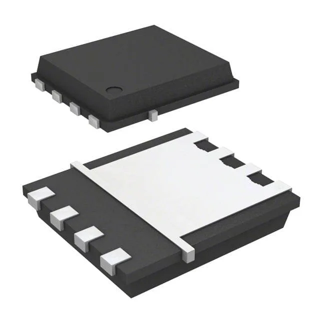
P-channel 30 V OptiMOS in a PG-TDSON-8-5
The Infineon BSC084P03NS3GATMA1 is a P-channel enhancement-mode MOSFET from the OptiMOS series, built on a trench MOSFET process. The continuous drain current is rated 14.9 A at 25°C ambient (Ta) and 78.6 A at the case (Tc), reflecting the thermal limit of the 8-PowerTDFN package versus the die capability. The 2.5 W (Ta) / 69 W (Tc) power dissipation split tells the buyer that a heatsink or board copper area is needed to approach the higher current rating.
Gate charge and drive voltage
Total gate charge Qg is 58 nC at Vgs = 10 V. At a 100 kHz switching frequency, the average gate-drive current is 5.8 mA — well within the capability of a standard MOSFET driver, but the 4785 pF input capacitance at 15 V Vds means the driver must source a peak current high enough to charge Ciss within the desired rise time. The drive voltage range for achieving the rated Rds(on) is 6 V to 10 V, with the 8.4 mOhm figure quoted at 10 V. At 6 V the on-resistance will be higher — the datasheet curve (not reproduced here) shows the typical increase. For designs running from a 5 V rail, the 3.1 V max threshold at 105 µA leaves little gate-drive margin; a 10 V supply is preferred for full performance.
ROHS3 compliant per the lifecycle record, with no exemptions that would block EU or Asian production lines.
The IPD50R950CEAUMA1 is a CoolMOS N-channel part in a different package and voltage class — not a functional replacement for a P-channel 30 V load switch.