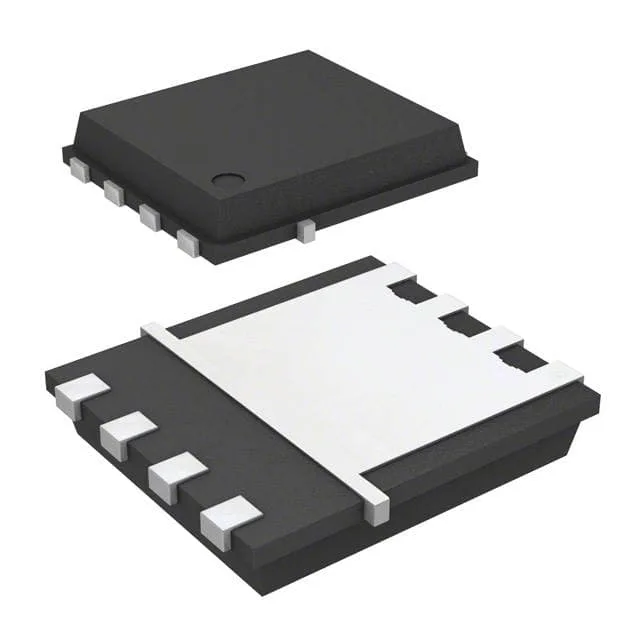
Infineon Technologies BSC059N04LS6ATMA1

BSC059N04LS6ATMA1 N-Channel 40 V MOSFET, 5.9 mOhm, OptiMOS

MPNBSC059N04LS6ATMA1
End of Life

Infineon OptiMOS™ BSC059N04LS6ATMA1, N-Channel MOSFET, 40 V Vds, 5.9 mOhm Rds(on) at 50 A, 9.4 nC gate charge, 8-PowerTDFN (PG-TDSON-8-6), -55°C to 175°C junction temperature.

$1.3Ref. price · indicative, final on quote
Packaging8-PowerTDFN
StockContact for availability
MOQ1 pcs
  • 100% new & originalTraceable channels only — no refurbs, no pulls, no remarked parts.
  • Date & lot codes on quoteStated per line before you commit; label photos on request.
  • MSL-compliant ESD packingMoisture-sealed bags with indicator cards; reels photo-verified.
  • PayPal buyer protectionPay by T/T, PayPal or Payoneer — card payments covered end to end.

Specifications

BSC059N04LS6ATMA1 Technical Specifications
ParameterValue
SeriesOptiMOS™
FET typeN-Channel
Mounting typeSurface Mount
Drain to source voltage40 V
Drive voltage (Max rds on, min rds on)4.5V, 10V
Current - continuous drain (Id) @ 25°C17A (Ta), 49A (Tc), 59A (Tc)
Power dissipation3W (Ta), 38W (Tc)
Operating temperature-55°C ~ 175°C (TJ)
PackageTape & Reel (TR); Cut Tape (CT)
Vgs±20V
TechnologyMOSFET (Metal Oxide)
Case8-PowerTDFN
Vgs(th) (Max) @ id2.3V @ 250µA
Rds on (Max) @ id, vgs5.9mOhm @ 50A, 10V
Gate charge (Qg) (Max) @ vgs9.4 nC @ 10 V
Input capacitance (Ciss) (Max) @ vds830 pF @ 20 V

Product details

What this 40 V OptiMOS N-channel brings to the switching node

The Infineon BSC059N04LS6ATMA1 is a 40 V N-channel MOSFET from the OptiMOS series, built for low-voltage synchronous rectification, DC-DC conversion, and motor-drive output stages. Its headline figure is a maximum on-resistance of 5.9 mOhm at 50 A drain current with a 10 V gate drive — that keeps conduction losses under control in a 49 A continuous drain current (case-rated) part. Gate charge is 9.4 nC at 10 V, which means the driver doesn't work hard to switch it fast. The 8-PowerTDFN package (PG-TDSON-8-6) is a surface-mount can with an exposed pad; the drain tab underneath pulls heat into the board copper. Junction temperature range spans -55°C to 175°C, so it handles hot environments like under-hood automotive or cramped power supplies without derating early.

Gate drive flexibility — 5 V logic or 10 V traditional

Drive voltage for minimum Rds(on) is 4.5 V and 10 V. Threshold voltage max is 2.3 V at 250 µA.

Capacitance and switching speed

Input capacitance (Ciss) is 830 pF at 20 V Vds. Gate charge is 9.4 nC at 10 V.

Lifecycle and sourcing

It is ROHS3 compliant. No end-of-life notice or last-time-buy window is in effect. For BOM planning, there is no immediate LTB risk.

Frequently asked questions

Does BSC059N04LS6ATMA1 work with 5 V gate drive?

Yes, the BSC059N04LS6ATMA1 specifies drive voltage down to 4.5 V for achieving near-minimum Rds(on), so a 5 V logic signal from a microcontroller or gate driver is sufficient to fully enhance the MOSFET.

Can BSC059N04LS6ATMA1 be used for motor control?

Yes, the 40 V drain-source rating, 49 A continuous drain current (case-rated), and 5.9 mOhm on-resistance make it suitable for low-voltage motor drive applications such as brushless DC motors in power tools, automotive actuators, and small pumps.

How does BSC059N04LS6ATMA1 compare to BSC059N04LS6?

The BSC059N04LS6ATMA1 is the same die in the same package as the BSC059N04LS6; the 'ATMA1' suffix indicates the tape-and-reel packaging variant. Electrical specifications are identical.