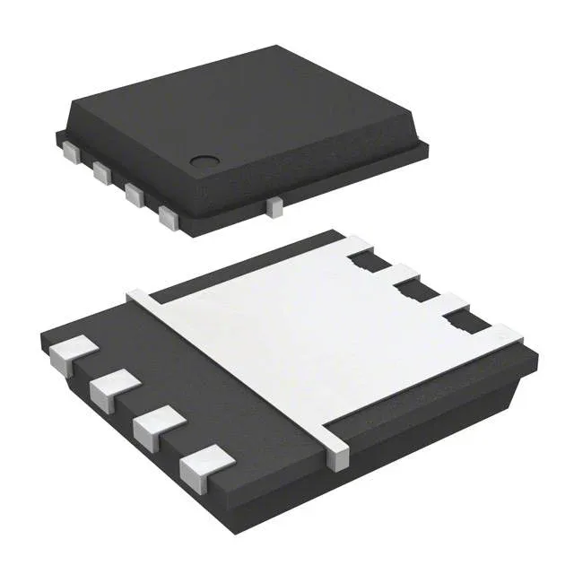
Infineon Technologies BSC050N04LSGATMA1

Infineon BSC050N04LSGATMA1 OptiMOS N-Ch 40V 5mOhm MOSFET

MPNBSC050N04LSGATMA1
End of Life

Infineon OptiMOS N-Channel MOSFET, 40 V drain-to-source, 5 mOhm Rds(on) at 50 A, 10 V gate drive, 85 A continuous drain at Tc, PG-TDSON-8-5 package, -55°C to 150°C junction temperature.

$0.91Ref. price · indicative, final on quote
Packaging8-PowerTDFN
RoHSROHS3 Compliant
SeriesOptiMOS™
Independent supplier — new & surplus stockAuthenticity-screened · ESD-safe packingListing updated Jul 2026

Specifications

BSC050N04LSGATMA1 specifications
ParameterValue
SeriesOptiMOS™
FET typeN-Channel
MountingSurface Mount
Drain to source voltage40 V
Drive voltage (Max rds on, min rds on)4.5V, 10V
Current - continuous drain (Id) @ 25°C18A (Ta), 85A (Tc)
Power dissipation2.5W (Ta), 57W (Tc)
Operating temperature-55°C ~ 150°C (TJ)
PackageTape & Reel (TR); Cut Tape (CT)
Vgs±20V
TechnologyMOSFET (Metal Oxide)
Case8-PowerTDFN
Vgs(th) (Max) @ id2V @ 27µA
Rds on (Max) @ id, vgs5mOhm @ 50A, 10V
Gate charge (Qg) (Max) @ vgs47 nC @ 10 V
Input capacitance (Ciss) (Max) @ vds3700 pF @ 20 V

Product details

The BSC050N04LSGATMA1: ROHS3 compliant, it fits RoHS-sensitive builds without exemption paperwork.

5 mOhm Rds(on) — what it buys in a 40 V power loop

For a 40 V rated part in a PG-TDSON-8-5 surface-mount package, that Rds(on) keeps conduction loss under 1.25 W at 50 A — a strong figure for a synchronous buck converter or a load switch where the duty cycle is high and the thermal budget is tight.

85 A continuous drain — thermal headroom in a small footprint

Rated 85 A continuous drain at case temperature (Tc) and 18 A at ambient (Ta) with a maximum power dissipation of 57 W at the case and 2.5 W in free air.

Gate drive and switching — 47 nC Qg at 10 V

The 47 nC figure means a standard gate-driver IC delivering 1 A peak can switch this MOSFET at roughly 100 kHz with acceptable switching losses. Drive voltage is specified for both 4.5 V and 10 V; at 4.5 V the Rds(on) will be higher than the 5 mOhm at 10 V, so confirm the driver rail before committing the BOM. The 2 V threshold maximum at 27 µA ensures the part turns on cleanly with logic-level gate signals.

Package and footprint — PG-TDSON-8-5

Supplied in the 8-lead PowerTDFN package (PG-TDSON-8-5), surface-mount with an exposed thermal pad. The package supports the 85 A drain rating when the pad is properly soldered to the PCB copper pour.

Frequently asked questions

What is the datasheet for BSC050N04LSG?

Design engineers need validation of electrical parameters and pinout before circuit integration.

What is the price of BSC050N04LSG?

Sourcing buyers compare costs across distributors to meet BOM budgets.

Is BSC050N04LSG in stock?

Availability directly affects production schedules and lead time decisions.

What is the equivalent or replacement for BSC050N04LSG?

Engineers and buyers need cross-reference options for second sourcing or obsolescence backup.

How to buy BSC050N04LSG in small quantities?

Prototype builders and maintenance techs seek low-volume purchase options without high MOQ.

Can BSC050N04LSG be used as a replacement for BSC050N04LSI?

Field replacement requires exact compatibility to avoid redesign or functional failure.