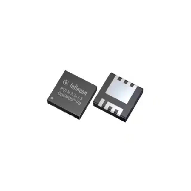
100 V, 140 A N-channel in a 8-PowerWDFN
The 72 nC total gate charge at 10 V sets the gate-drive power requirement; at a 100 kHz switching frequency the driver must supply about 7.2 mA average current just to charge and discharge the gate capacitance.
Thermal and switching headroom
Input capacitance is 5300 pF at 50 V drain-source; this capacitance must be charged and discharged each switching cycle, contributing to the driver's dynamic current demand and the switching losses in hard-switched topologies.
The OptiMOS™ 5 family includes multiple voltage and Rds(on) variants in the same PG-WSON-8-2 footprint, allowing a pin-compatible upgrade path if the current rating or on-resistance requirement changes during the design cycle.