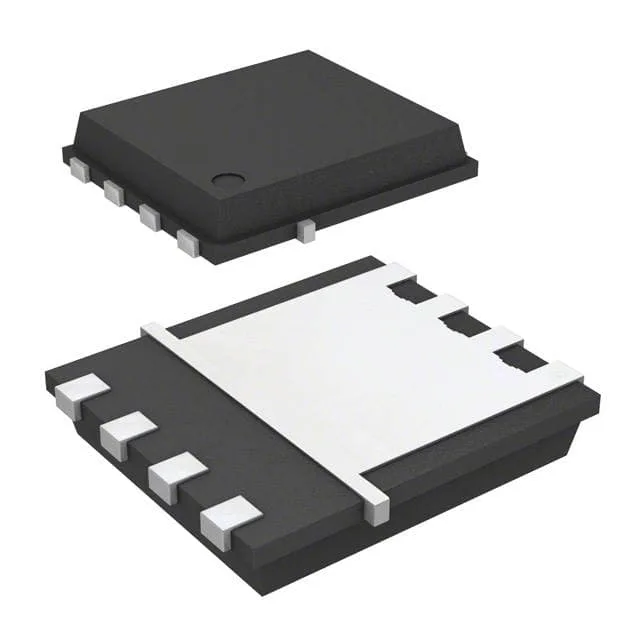
Infineon Technologies BSC034N06NSATMA1

Infineon BSC034N06NSATMA1 OptiMOS N-Channel MOSFET, 60V 100A

MPNBSC034N06NSATMA1
End of Life

Infineon OptiMOS N-Channel MOSFET, 60V drain-source, 100A continuous drain, 3.4 mOhm Rds(on) at 10V, PG-TDSON-8-7 package, -55 to 150°C junction temperature.

$2.18Ref. price · indicative, final on quote
Packaging8-PowerTDFN
StockContact for availability
MOQ1 pcs
  • 100% new & originalTraceable channels only — no refurbs, no pulls, no remarked parts.
  • Date & lot codes on quoteStated per line before you commit; label photos on request.
  • MSL-compliant ESD packingMoisture-sealed bags with indicator cards; reels photo-verified.
  • PayPal buyer protectionPay by T/T, PayPal or Payoneer — card payments covered end to end.

Specifications

BSC034N06NSATMA1 Technical Specifications
ParameterValue
SeriesOptiMOS™
FET typeN-Channel
Mounting typeSurface Mount
Drain to source voltage60 V
Drive voltage (Max rds on, min rds on)6V, 10V
Current - continuous drain (Id) @ 25°C100A (Tc)
Power dissipation2.5W (Ta), 74W (Tc)
Operating temperature-55°C ~ 150°C (TJ)
PackageTape & Reel (TR); Cut Tape (CT)
Vgs±20V
TechnologyMOSFET (Metal Oxide)
Case8-PowerTDFN
Vgs(th) (Max) @ id3.3V @ 41µA
Rds on (Max) @ id, vgs3.4mOhm @ 50A, 10V
Gate charge (Qg) (Max) @ vgs41 nC @ 10 V
Input capacitance (Ciss) (Max) @ vds3000 pF @ 30 V

Product details

On-resistance and gate charge — what they mean for the switching stage

The BSC034N06NSATMA1: The 3.4 mOhm maximum Rds(on) at 50 A and 10 V gate drive keeps conduction losses low in high-current paths. The 41 nC total gate charge at 10 V sets the switching energy. The drive voltage range of 6 V to 10 V means it can be driven from a standard 10 V gate-drive rail, but also works with 6 V logic-level outputs if the application can tolerate the slightly higher Rds(on) at reduced gate voltage.

Package and mounting — PG-TDSON-8-7

The PG-TDSON-8-7 package is a 8-lead PowerTDFN with an exposed drain pad on the bottom. The pad must be soldered to a copper land on the PCB with adequate thermal vias to the inner ground plane; the datasheet's recommended footprint and thermal via pattern should be followed to achieve the rated 74 W power dissipation at the case. The part is surface-mount only, so reflow soldering is the intended assembly method. The supplier device package code PG-TDSON-8-7 is Infineon's internal designation; the industry-standard package name is 8-PowerTDFN.

Active production, no end-of-life concern

The BSC034N06NSATMA1 carries an Active lifecycle status from Infineon. There is no last-time-buy notice or NRND flag on this part. It is ROHS3 compliant, which covers the current EU RoHS exemption list. For new designs, this part is a safe choice without near-term obsolescence risk. The OptiMOS series is a mature, widely used platform, and Infineon typically provides long-term support for these parts.

Frequently asked questions

What is the closest pin-compatible alternative to BSC034N06NSATMA1 in this component family?

Within the OptiMOS family, Infineon offers several 60 V N-channel MOSFETs in the same PG-TDSON-8-7 footprint. The BSC034N06NSATMA1 is distinguished by its 3.4 mOhm Rds(on) and 41 nC gate charge. A lower Rds(on) sibling (e.g., BSC028N06NS) would have a different gate-charge trade-off; a higher Rds(on) version would have lower gate charge. The choice depends on the balance between conduction loss and switching speed in your application. No single drop-in equivalent exists across all operating points.

Is BSC034N06NSATMA1 RoHS compliant?

Yes, it is ROHS3 compliant, meeting the latest EU RoHS directive including the exemption for lead in high-melting-temperature solders.