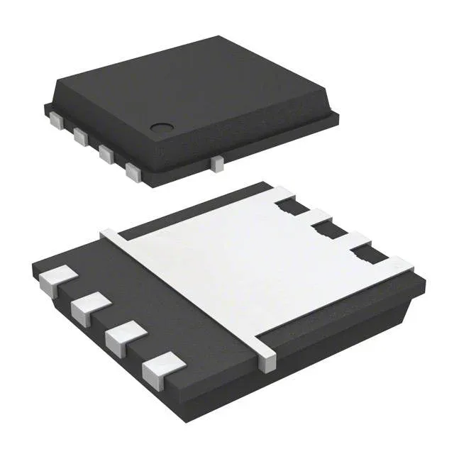
Infineon Technologies BSC032NE2LSATMA1

Infineon BSC032NE2LSATMA1 N-Channel MOSFET, 25V, 3.2mOhm

MPNBSC032NE2LSATMA1
End of Life

Infineon OptiMOS™ BSC032NE2LSATMA1, N-Channel MOSFET, 25V Vdss, 3.2mOhm Rds(on) @ 10V, 22A (Ta) / 84A (Tc) continuous drain, 16nC gate charge, 8-PowerTDFN (PG-TDSON-8-6), -55°C to 150°C junction.

$0.95Ref. price · indicative, final on quote
Packaging8-PowerTDFN
StockContact for availability
MOQ1 pcs
  • 100% new & originalTraceable channels only — no refurbs, no pulls, no remarked parts.
  • Date & lot codes on quoteStated per line before you commit; label photos on request.
  • MSL-compliant ESD packingMoisture-sealed bags with indicator cards; reels photo-verified.
  • PayPal buyer protectionPay by T/T, PayPal or Payoneer — card payments covered end to end.

Specifications

BSC032NE2LSATMA1 Technical Specifications
ParameterValue
SeriesOptiMOS™
FET typeN-Channel
Mounting typeSurface Mount
Drain to source voltage25 V
Drive voltage (Max rds on, min rds on)4.5V, 10V
Current - continuous drain (Id) @ 25°C22A (Ta), 84A (Tc)
Power dissipation2.8W (Ta), 78W (Tc)
Operating temperature-55°C ~ 150°C (TJ)
PackageTape & Reel (TR); Cut Tape (CT)
Vgs±20V
TechnologyMOSFET (Metal Oxide)
Case8-PowerTDFN
Vgs(th) (Max) @ id2V @ 250µA
Rds on (Max) @ id, vgs3.2mOhm @ 30A, 10V
Gate charge (Qg) (Max) @ vgs16 nC @ 10 V
Input capacitance (Ciss) (Max) @ vds1200 pF @ 12 V

Product details

What the BSC032NE2LSATMA1 is and where it fits

The Infineon BSC032NE2LSATMA1 is a 25 V N-channel MOSFET from the OptiMOS™ series, built on a metal-oxide trench technology. It delivers a maximum Rds(on) of 3.2 mOhm at 10 V gate drive with 30 A drain current — a figure that puts it in the low-loss tier for a 25 V part. The die is rated for 84 A continuous drain when the case temperature is held at 25°C, but the same silicon in free air (Ta) is limited to 22 A because the 8-PowerTDFN package (PG-TDSON-8-6) can only shed 2.8 W to the ambient without a heatsink. That split tells you: this MOSFET is designed for a board that can conduct heat away through the PCB copper, not for a standalone through-hole part bolted to a fin. Typical applications include synchronous rectification in DC-DC converters, load switches in telecom and server power rails, and battery protection in power tools or e-mobility gear. The 150°C junction rating and ±20 V maximum gate voltage give it margin in environments where transients and thermal cycling are routine — automotive under-hood, industrial motor drives, and outdoor telecom enclosures.

Package and thermal reality

The 8-PowerTDFN (PG-TDSON-8-6) is a surface-mount package with an exposed drain pad on the bottom. The 2.8 W maximum dissipation at 25°C ambient assumes the standard JEDEC board with minimal copper — real designs should expect to need multiple vias to an inner-layer copper plane to keep the junction below 150°C at high current. The 78 W case-temperature rating is only achievable with the drain pad soldered to a substantial heatsink or PCB thermal plane. For a 22 A continuous load in still air, verify the board's thermal resistance; the MOSFET itself can handle the current, but the board must sink the heat.

Lifecycle and sourcing posture

No last-time-buy notice or end-of-life window is on record. The part is available through independent distribution; pricing and stock are confirmed at quote time against an RFQ.

Frequently asked questions

What is the Rds(on) of BSC032NE2LSATMA1?

The maximum Rds(on) is 3.2 mOhm at 30 A drain current with a 10 V gate drive. At 4.5 V gate drive the on-resistance is higher; the datasheet typical curve shows the value, but the guaranteed maximum is specified only at 10 V.

What package is BSC032NE2LSATMA1?

The BSC032NE2LSATMA1 is supplied in an 8-PowerTDFN package, also designated PG-TDSON-8-6 by Infineon. It is a surface-mount package with an exposed drain pad for thermal management.

Is BSC032NE2LSATMA1 RoHS compliant?

Yes, Infineon lists the BSC032NE2LSATMA1 as ROHS3 compliant.