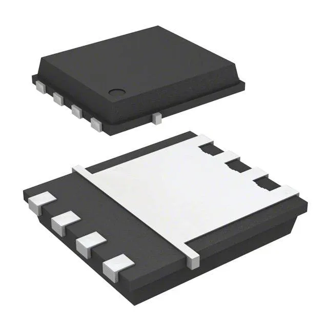
Infineon Technologies BSC030N08NS5ATMA1

Infineon BSC030N08NS5ATMA1 OptiMOS N-Channel MOSFET

MPNBSC030N08NS5ATMA1
End of Life

Infineon OptiMOS N-Channel MOSFET, 80 V, 100 A, 3 mOhm Rds(on) at 10 V, 76 nC gate charge, -55 to 150 °C, PG-TDSON-8-7 surface mount.

$2.24Ref. price · indicative, final on quote
Packaging8-PowerTDFN
StockContact for availability
MOQ1 pcs
  • 100% new & originalTraceable channels only — no refurbs, no pulls, no remarked parts.
  • Date & lot codes on quoteStated per line before you commit; label photos on request.
  • MSL-compliant ESD packingMoisture-sealed bags with indicator cards; reels photo-verified.
  • PayPal buyer protectionPay by T/T, PayPal or Payoneer — card payments covered end to end.

Specifications

BSC030N08NS5ATMA1 Technical Specifications
ParameterValue
SeriesOptiMOS™
FET typeN-Channel
Mounting typeSurface Mount
Drain to source voltage80 V
Drive voltage (Max rds on, min rds on)6V, 10V
Current - continuous drain (Id) @ 25°C100A (Tc)
Power dissipation2.5W (Ta), 139W (Tc)
Operating temperature-55°C ~ 150°C (TJ)
PackageTape & Reel (TR); Cut Tape (CT)
Vgs±20V
TechnologyMOSFET (Metal Oxide)
Case8-PowerTDFN
Vgs(th) (Max) @ id3.8V @ 95µA
Rds on (Max) @ id, vgs3mOhm @ 50A, 10V
Gate charge (Qg) (Max) @ vgs76 nC @ 10 V
Input capacitance (Ciss) (Max) @ vds5600 pF @ 40 V

Product details

OptiMOS 80 V N-channel for high-efficiency power switching

The BSC030N08NS5ATMA1: Gate charge of 76 nC at 10 V and input capacitance of 5600 pF at 40 V Vds define the switching-speed budget — the gate driver must supply that charge per cycle, so the switching frequency and driver strength need to be matched to avoid excessive cross-conduction or slow edges. The junction temperature range of -55 to 150 °C suits industrial motor drives, automotive under-hood, and telecom rectifiers. The 2.5 W (Ta) / 139 W (Tc) power dissipation limits require a well-designed thermal path.

Gate drive and switching considerations

The device specifies drive voltage for minimum Rds(on) at 10 V, with a threshold of 3.8 V maximum at 95 µA. A 6 V drive reduces Rds(on) slightly but not to the full 3 mOhm — 10 V is the target for rated conduction. The ±20 V Vgs max means the gate must be clamped in systems where the gate-drive supply can overshoot, particularly during startup or fault events. Input capacitance of 5600 pF at 40 V Vds means the gate driver sees a moderate capacitive load. The 76 nC gate charge at 10 V gives the total energy per cycle.

Lifecycle and sourcing

The BSC030N08NS5ATMA1 carries an Active lifecycle status from Infineon, with ROHS3 compliance. No end-of-life notice or last-time-buy window is in effect, so the part is suitable for new designs and production ramps without immediate obsolescence risk.

Frequently asked questions

What is the lead time for BSC030N08NS5ATMA1?

Lead time is confirmed at quote time against an RFQ. Current market conditions affect lead times — submit an RFQ for your quantity and target delivery date.