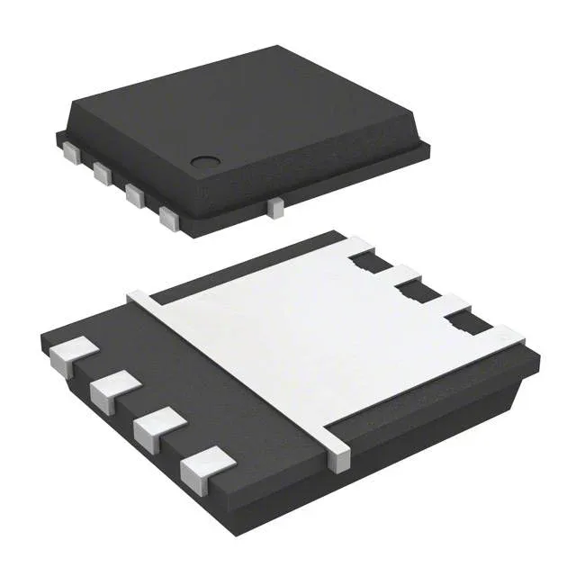
Infineon Technologies BSC028N06NSSCATMA1

Infineon BSC028N06NSSCATMA1 OptiMOS N-Ch 60V 100A MOSFET

MPNBSC028N06NSSCATMA1
End of Life

Infineon OptiMOS N-Channel MOSFET, BSC028N06NSSCATMA1, 60V Vdss, 100A Id, 2.8mOhm Rds(on) at 50A, PG-TDSON-8-7, -55°C to 150°C.

$2.49Ref. price · indicative, final on quote
Packaging8-PowerTDFN
StockContact for availability
MOQ1 pcs
  • 100% new & originalTraceable channels only — no refurbs, no pulls, no remarked parts.
  • Date & lot codes on quoteStated per line before you commit; label photos on request.
  • MSL-compliant ESD packingMoisture-sealed bags with indicator cards; reels photo-verified.
  • PayPal buyer protectionPay by T/T, PayPal or Payoneer — card payments covered end to end.

Specifications

BSC028N06NSSCATMA1 Technical Specifications
ParameterValue
SeriesOptiMOS™
FET typeN-Channel
Mounting typeSurface Mount
Drain to source voltage60 V
Drive voltage (Max rds on, min rds on)6V, 10V
Current - continuous drain (Id) @ 25°C100A (Tc)
Power dissipation2.5W (Ta), 83W (Tc)
Operating temperature-55°C ~ 150°C (TJ)
PackageTape & Reel (TR); Cut Tape (CT)
Vgs±20V
TechnologyMOSFET (Metal Oxide)
Case8-PowerTDFN
Vgs(th) (Max) @ id3.3V @ 50µA
Rds on (Max) @ id, vgs2.8mOhm @ 50A, 10V
Gate charge (Qg) (Max) @ vgs49 nC @ 10 V
Input capacitance (Ciss) (Max) @ vds3375 pF @ 30 V

Product details

The Infineon BSC028N06NSSCATMA1 is an OptiMOS N-channel power MOSFET rated for 60 V drain-to-source and 100 A continuous drain current at case temperature 25 °C. At 50 A the dissipation in the FET is about 7 W at 25 °C junction; the package is rated for 83 W at the case, so the thermal limit is set by the board copper and airflow, not the silicon. The gate charge is 49 nC at 10 V. For a 100 kHz switching frequency the average gate-drive current works out to about 4.9 mA — well within a standard driver's capability, but the peak current needed to switch the gate in tens of nanoseconds is what sizes the driver output stage. The input capacitance is 3375 pF at 30 V Vds, which sets the switching loss slope on the Miller plateau.

Temperature range and field environment

The junction temperature range is -55 °C to 150 °C. That is the full automotive and industrial envelope — under-hood electronics, outdoor telecom cabinets, motor drives in factory-floor enclosures. The 150 °C ceiling means the Rds(on) derating curve matters more than the room-temperature number; at 125 °C junction the on-resistance roughly doubles from the 25 °C value, so the thermal design should budget for about 5.6 mOhm at the hot end.

Package and mounting — not a field-swap part

The package is an 8-PowerTDFN, supplier code PG-TDSON-8-7. This is not a part you swap on site with a soldering iron — the exposed pad needs a hot-air station or reflow profile. The mounting type is surface mount, and the gate threshold is 3.3 V max at 50 µA, so a 5 V logic gate drive will turn it on hard enough to hit the rated Rds(on) with 6 V or 10 V drive.

Lifecycle and compliance

It is ROHS3 compliant, and the series is OptiMOS, Infineon's established low-voltage power MOSFET family.

Frequently asked questions

What is the Rds(on) of BSC028N06NSSCATMA1?

This is the room-temperature spec; at 150 °C junction the Rds(on) approximately doubles, so the hot-end design should budget for about 5.6 mOhm.

Is BSC028N06NSSCATMA1 lead-free?

Yes, it is ROHS3 compliant, which restricts lead and other hazardous substances. The part is suitable for lead-free soldering processes.

Can IPD50R950CEAUMA1 replace BSC028N06NSSCATMA1?

No. IPD50R950CEAUMA1 is a 500 V CoolMOS CE device — a completely different voltage class. The BSC028N06NSSCATMA1 is a 60 V OptiMOS part. They are not functional equivalents or pin-compatible replacements.