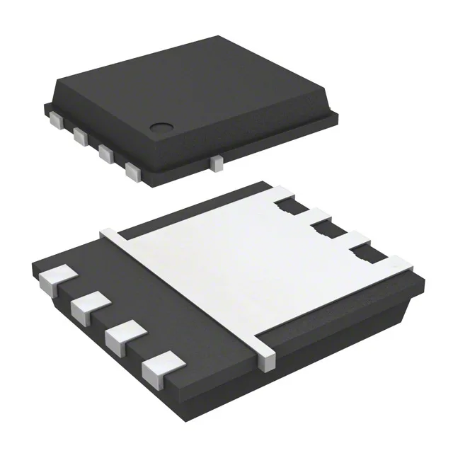
Infineon Technologies BSC027N04LSGATMA1

Infineon BSC027N04LSGATMA1 N-Channel MOSFET, 40 V, 100 A

MPNBSC027N04LSGATMA1
End of Life

Infineon OptiMOS BSC027N04LSGATMA1, N-channel MOSFET, 40 V drain-source voltage, 100 A continuous drain at case temperature, 2.7 mOhm max on-resistance at 50 A, 10 V gate drive, PG-TDSON-8-1 package, -55°C to 150°C junction temperature.

$1.52Ref. price · indicative, final on quote
Packaging8-PowerTDFN
StockContact for availability
MOQ1 pcs
  • 100% new & originalTraceable channels only — no refurbs, no pulls, no remarked parts.
  • Date & lot codes on quoteStated per line before you commit; label photos on request.
  • MSL-compliant ESD packingMoisture-sealed bags with indicator cards; reels photo-verified.
  • PayPal buyer protectionPay by T/T, PayPal or Payoneer — card payments covered end to end.

Specifications

BSC027N04LSGATMA1 Technical Specifications
ParameterValue
SeriesOptiMOS™
FET typeN-Channel
Mounting typeSurface Mount
Drain to source voltage40 V
Drive voltage (Max rds on, min rds on)4.5V, 10V
Current - continuous drain (Id) @ 25°C24A (Ta), 100A (Tc)
Power dissipation2.5W (Ta), 83W (Tc)
Operating temperature-55°C ~ 150°C (TJ)
PackageTape & Reel (TR); Cut Tape (CT)
Vgs±20V
TechnologyMOSFET (Metal Oxide)
Case8-PowerTDFN
Vgs(th) (Max) @ id2V @ 49µA
Rds on (Max) @ id, vgs2.7mOhm @ 50A, 10V
Gate charge (Qg) (Max) @ vgs85 nC @ 10 V
Input capacitance (Ciss) (Max) @ vds6800 pF @ 20 V

Product details

40 V, 100 A N-channel — what the ratings mean for the power stage

The Infineon BSC027N04LSGATMA1 is an OptiMOS N-channel MOSFET rated for 40 V drain-source voltage and a continuous drain current of 100 A at the case temperature, with a maximum on-resistance of 2.7 mOhm at 50 A and 10 V gate drive. The 83 W package limit at Tc can handle the dissipation with adequate heatsinking. The 24 A rating at ambient temperature (Ta) is the board-limited, no-heatsink ceiling. Gate charge is 85 nC at 10 V. A gate driver capable of sourcing and sinking a few amps will keep switching losses manageable. If the design drives the gate at 4.5 V instead of 10 V, expect the on-resistance to rise above the 2.7 mOhm minimum.

Package and mounting — PG-TDSON-8-1

The part comes in an 8-PowerTDFN package, supplier device code PG-TDSON-8-1, which is a surface-mount, dual-side-cooled package. The exposed drain pad on the bottom requires a thermal via pattern on the PCB to transfer heat to the ground plane. The 6800 pF input capacitance at 20 V Vds means the gate driver sees a moderate capacitive load — keep the gate loop short to avoid ringing.

Lifecycle and sourcing

The BSC027N04LSGATMA1 carries an active lifecycle status with ROHS3 compliance.

Frequently asked questions

What is the datasheet for BSC027N04LSGATMA1?

Engineers need detailed electrical characteristics and package info for design validation.

Where to buy BSC027N04LSGATMA1?

Sourcing buyers need to check stock, price, and lead times across distributors.

What is the price of BSC027N04LSGATMA1?

Cost is key for BOM budgeting and cost-down analysis.

Is BSC027N04LSGATMA1 equivalent to BSC028N04LS?

Finding direct replacements or alternatives ensures design flexibility and supply continuity.

What is the pinout of BSC027N04LSGATMA1?

Critical for PCB layout and ensuring correct connections in the circuit.

Is BSC027N04LSGATMA1 obsolete?

Lifecycle status determines long-term availability for production and maintenance.