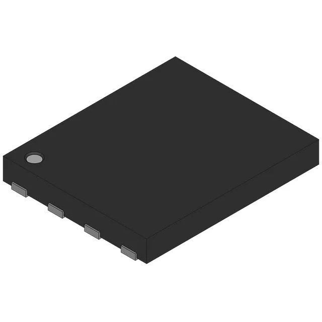
Infineon Technologies BSC026N02KSG — Logic ICs

Infineon BSC026N02KSG OptiMOS™2 N-Channel MOSFET, 20 V

MPNBSC026N02KSG
End of Life

Infineon OptiMOS™2 N-Channel MOSFET, 20 V Vds, 2.6 mΩ Rds(on) at 4.5 V, 134 A continuous drain, PG-TDSON-8-1 package, -55°C to 150°C junction temperature.

$0.76Ref. price · indicative, final on quote
Packaging8-PowerTDFN
StockContact for availability
MOQ1 pcs
  • 100% new & originalTraceable channels only — no refurbs, no pulls, no remarked parts.
  • Date & lot codes on quoteStated per line before you commit; label photos on request.
  • MSL-compliant ESD packingMoisture-sealed bags with indicator cards; reels photo-verified.
  • PayPal buyer protectionPay by T/T, PayPal or Payoneer — card payments covered end to end.

Specifications

BSC026N02KSG Technical Specifications
ParameterValue
SeriesOptiMOS™2
FET typeN-Channel
Mounting typeSurface Mount
Drain to source voltage20 V
Drive voltage (Max rds on, min rds on)2.5V, 4.5V
Current - continuous drain (Id) @ 25°C25A (Ta), 134A (Tc)
Power dissipation2.8W (Ta), 78W (Tc)
Operating temperature-55°C ~ 150°C (TJ)
PackageBulk
Vgs±12V
TechnologyMOSFET (Metal Oxide)
Case8-PowerTDFN
Vgs(th) (Max) @ id1.2V @ 200µA
Rds on (Max) @ id, vgs2.6mOhm @ 50A, 4.5V
Gate charge (Qg) (Max) @ vgs52.7 nC @ 4.5 V
Input capacitance (Ciss) (Max) @ vds7800 pF @ 10 V

Product details

2.6 mΩ at 4.5 V — logic-level gate drive without the headroom tax

The BSC026N02KSG: The 2.6 mΩ maximum on-resistance at 4.5 V gate drive with 50 A is a logic-level threshold that lets a PWM signal from an MCU or gate driver turn the FET fully on without a secondary gate boost. The minimum drive voltage for the lowest Rds(on) is 2.5 V.

Infineon lists the BSC026N02KSG as Active in its product portfolio.

Package and thermal: PG-TDSON-8-1

Housed in an 8-lead PowerTDFN (Infineon's PG-TDSON-8-1), this is a surface-mount package with an exposed drain pad for heat sinking. The thermal resistance splits: 2.8 W maximum dissipation at ambient (Ta) but 78 W at the case (Tc), meaning the board's copper area and via stitching under the pad determine real-world current capability. The 134 A continuous drain rating at 25°C case temperature assumes a well-thermalized layout; at ambient with no heatsink the current is derated to 25 A.

Switching and drive numbers

Gate charge is 52.7 nC at 4.5 V, and input capacitance sits at 7800 pF at 10 V drain. The driver needs to source and sink enough peak current to switch the gate through the Miller plateau without excessive slew.

Frequently asked questions

What is the datasheet for BSC026N02KSG?

Design engineers and buyers need official specs (Rds(on), Vdss, gate charge) to validate fit in schematic or BOM.

How much does BSC026N02KSG cost per unit in 1000-piece quantities?

Sourcing buyers need real price breaks to compare with alternatives and budget BOM lines.

Where can I buy BSC026N02KSG with stock?

Buyers and engineers need immediate availability from distributors to avoid production delays.

What is the equivalent replacement for BSC026N02KSG?

Maintenance techs and brokers need to find cross-reference or drop-in substitute if the part is allocated or obsolete.

Is BSC026N02KSG obsolete or still in production?

Brokers and long-term planners must know lifecycle status to avoid future supply risk.

What is the package and pinout of BSC026N02KSG?

Engineers verifying PCB layout require exact package (PG-TDSON-8) dimensions and pin assignment.