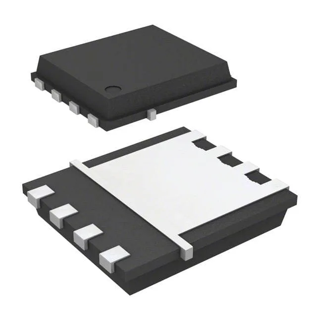
The Infineon BSC015NE2LS5IATMA1 is an N-channel OptiMOS™ power MOSFET rated for 25 V drain-to-source and 100 A continuous drain current when the case is held at 25°C. The 1.5 mOhm maximum on-resistance at 10 V gate drive and 30 A load is the headline figure.
Gate drive and switching — what to budget
Gate charge is 30 nC at 10 V, and the drive voltage range for rated Rds(on) is 4.5 V to 10 V. That 30 nC is modest — a typical gate driver can switch it in tens of nanoseconds — but the input capacitance of 2000 pF at 12 V Vds means the driver must source enough peak current to avoid slow edges and extra switching loss. The ±16 V Vgs maximum gives headroom for gate-drive overshoot, but stay within the 4.5 V to 10 V window for the on-resistance numbers in the spec table.
Surface-mount only. The 2.5 W at ambient is the limit with minimal copper; plan the layout accordingly.
The 150°C maximum junction means the part can handle brief overloads, but continuous operation near that limit requires careful thermal design — the 50 W Tc rating assumes the case is held at 25°C, which is not realistic in a hot enclosure.