The BSC014N04LSIATMA1: The 8-PowerTDFN package has an exposed drain pad underneath. That pad is the main thermal path — the datasheet calls for a soldered copper land on the PCB with thermal vias to inner layers. Rework is doable with hot air if you preheat the board from the back side to avoid lifting the pad. The package body is low-profile, which helps in dense layouts but means the solder joints under the part are hard to inspect visually — X-ray or a borescope is your friend for a production run.
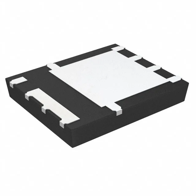
Infineon BSC014N04LSIATMA1 OptiMOS N-Ch MOSFET, 40V 100A
MPNBSC014N04LSIATMA1
End of Life
Infineon OptiMOS™ N-Channel MOSFET, 40 V drain-to-source voltage, 31 A (Ta) / 100 A (Tc) continuous drain current, 1.45 mOhm max on-resistance at 10 V, PG-TDSON-8 FL package, -55°C to 150°C junction temperature.
$2.96Ref. price · indicative, final on quote
Packaging8-PowerTDFN
RoHSROHS3 Compliant
SeriesOptiMOS™
Independent supplier — new & surplus stockAuthenticity-screened · ESD-safe packingListing updated Jul 2026
Specifications
| Parameter | Value |
|---|---|
| Series | OptiMOS™ |
| FET type | N-Channel |
| Mounting | Surface Mount |
| Drain to source voltage | 40 V |
| Drive voltage (Max rds on, min rds on) | 4.5V, 10V |
| Current - continuous drain (Id) @ 25°C | 31A (Ta), 100A (Tc) |
| Power dissipation | 2.5W (Ta), 96W (Tc) |
| Operating temperature | -55°C ~ 150°C (TJ) |
| Package | Tape & Reel (TR); Cut Tape (CT) |
| Vgs | ±20V |
| Technology | MOSFET (Metal Oxide) |
| Case | 8-PowerTDFN |
| Vgs(th) (Max) @ id | 2V @ 250µA |
| Rds on (Max) @ id, vgs | 1.45mOhm @ 50A, 10V |
| Gate charge (Qg) (Max) @ vgs | 55 nC @ 10 V |
| Input capacitance (Ciss) (Max) @ vds | 4000 pF @ 20 V |
Product details
Frequently asked questions
Is BSC014N04LSIATMA1 RoHS compliant?
Yes, it is ROHS3 compliant.
What is the closest functional second-source for BSC014N04LSIATMA1?
The IPD50R950CEAUMA1 is a different-class part — a 500 V CoolMOS with 950 mOhm Rds(on) and 4.3 A current rating. It is not a functional substitute for this 40 V, 100 A OptiMOS. For a true second-source, look for another 40 V N-channel MOSFET in a similar PowerTDFN package with Rds(on) near 1.45 mOhm and gate charge around 55 nC.