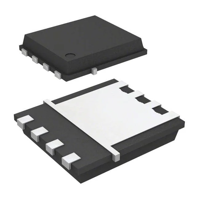
Infineon Technologies BSC009NE2LS5ATMA1

Infineon BSC009NE2LS5ATMA1 OptiMOS N-Ch 25V MOSFET

MPNBSC009NE2LS5ATMA1
End of Life

Infineon OptiMOS 5 BSC009NE2LS5ATMA1, N-Channel MOSFET, 25 V Vdss, 0.9 mOhm Rds(on) at 30 A/10 V, 57 nC Qg, 41 A (Ta) / 100 A (Tc), PG-TDSON-8-7, -55 to 150 °C.

$2.5Ref. price · indicative, final on quote
Packaging8-PowerTDFN
StockContact for availability
MOQ1 pcs
  • 100% new & originalTraceable channels only — no refurbs, no pulls, no remarked parts.
  • Date & lot codes on quoteStated per line before you commit; label photos on request.
  • MSL-compliant ESD packingMoisture-sealed bags with indicator cards; reels photo-verified.
  • PayPal buyer protectionPay by T/T, PayPal or Payoneer — card payments covered end to end.

Specifications

BSC009NE2LS5ATMA1 Technical Specifications
ParameterValue
SeriesOptiMOS™
FET typeN-Channel
Mounting typeSurface Mount
Drain to source voltage25 V
Drive voltage (Max rds on, min rds on)4.5V, 10V
Current - continuous drain (Id) @ 25°C41A (Ta), 100A (Tc)
Power dissipation2.5W (Ta), 74W (Tc)
Operating temperature-55°C ~ 150°C (TJ)
PackageTape & Reel (TR); Cut Tape (CT)
Vgs±16V
TechnologyMOSFET (Metal Oxide)
Case8-PowerTDFN
Vgs(th) (Max) @ id2V @ 250µA
Rds on (Max) @ id, vgs0.9mOhm @ 30A, 10V
Gate charge (Qg) (Max) @ vgs57 nC @ 10 V
Input capacitance (Ciss) (Max) @ vds3900 pF @ 12 V

Product details

0.9 mOhm Rds(on) — the 25°C headline and the hot reality

The Infineon BSC009NE2LS5ATMA1 is an OptiMOS 5 N-channel MOSFET rated for 25 V drain-to-source voltage with a typical on-resistance of 0.9 mOhm at 30 A drain current and 10 V gate drive. That 0.9 mOhm figure is at 25°C junction — at 125°C junction the Rds(on) roughly doubles, so budget 1.8 mOhm for conduction loss calculations under hot operating conditions. The 57 nC total gate charge at 10 V means a 100 kHz switching frequency draws about 5.7 mA average from the gate driver, which is manageable for most half-bridge drivers but the peak current capability still needs checking against the driver's source/sink rating.

Dual current rating: 41 A vs 100 A — the package is the bottleneck

The continuous drain current is listed as 41 A at 25°C ambient (Ta) and 100 A at 25°C case (Tc). That spread tells you the PG-TDSON-8-7 package is the thermal limiter, not the silicon die. Without a heatsink path to the package tab, the 41 A Ta rating is the practical ceiling. The 74 W power dissipation at Tc vs 2.5 W at Ta reinforces the same point — this MOSFET needs a thermal interface to the PCB copper or an external heatsink to run anywhere near its die capability.

Infineon lists the BSC009NE2LS5ATMA1 as Active in production. No end-of-life notice, no last-time-buy deadline. The part is ROHS3 compliant.

Package and footprint: PG-TDSON-8-7

The supplier device package is PG-TDSON-8-7, a surface-mount 8-pin PowerTDFN. The 8-pin pitch and pad layout are standard for this Infineon OptiMOS 5 family, so a layout from a sibling part like the BSC009NE2LS5I should transfer with minor adjustments.

Frequently asked questions

What is the Rds(on) of BSC009NE2LS5ATMA1?

The maximum Rds(on) is 0.9 mOhm at 30 A drain current and 10 V gate drive, measured at 25°C junction. At hot junction temperatures (125°C) the on-resistance approximately doubles, so budget around 1.8 mOhm for conduction loss calculations under continuous high-current operation.

Is BSC009NE2LS5ATMA1 RoHS compliant and lead-free?

Yes, Infineon lists this part as ROHS3 Compliant. It meets the EU RoHS directive for lead-free and restricted-substance compliance.