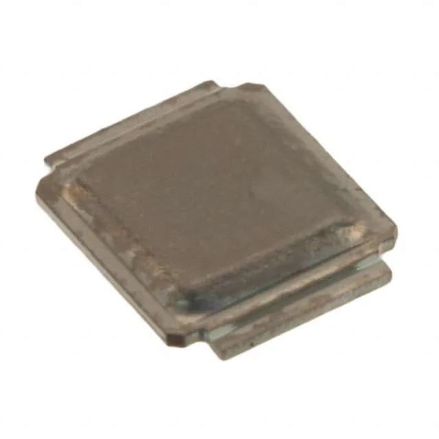
60 V, 2.8 mOhm — the conduction-loss floor
The Infineon BSB028N06NN3GXUMA1 is an N-channel OptiMOS power MOSFET rated for 60 V drain-source breakdown and a continuous drain current of 90 A at the case (Tc) or 22 A at ambient (Ta).
Total gate charge is 143 nC at Vgs = 10 V, with an input capacitance of 12000 pF at Vds = 30 V. The 2.2 W maximum dissipation at ambient (Ta) versus 78 W at the case (Tc) tells the layout engineer that the thermal path through the CanPAK M package's large solder pad is the primary heat-removal route; the PCB copper area under the pad sets the real junction temperature.
The MG-WDSON-2 CanPAK M package is a surface-mount design with a large exposed drain pad for soldering directly to the PCB copper.
It is ROHS3 compliant.