8 GHz fT and 19 dB gain — the RF front-end fit
The BFS483H6327XTSA1: The 8 GHz transition frequency puts this transistor solidly into the UHF and low-microwave band — 900 MHz GSM, 1.8 GHz DCS, 2.4 GHz ISM, and 5 GHz WLAN front-ends are all within its gain bandwidth. The 19 dB gain figure is the forward transmission coefficient (S21) at the manufacturer's specified bias point; in a single-stage common-emitter LNA, that translates to roughly 17–18 dB of usable gain after matching network losses. Noise figure runs 0.9 dB typical at 900 MHz and 1.4 dB at 1.8 GHz — low enough for a receiver front-end where every tenth of a dB of NF directly adds to the system noise floor. The 65 mA maximum collector current and 12 V collector-emitter breakdown cover the bias range for a typical small-signal LNA or oscillator buffer; you are not pushing the SOA limits at 5–10 mA and 3–5 V.
Dual NPN in SOT-363 — board-level fit and rework
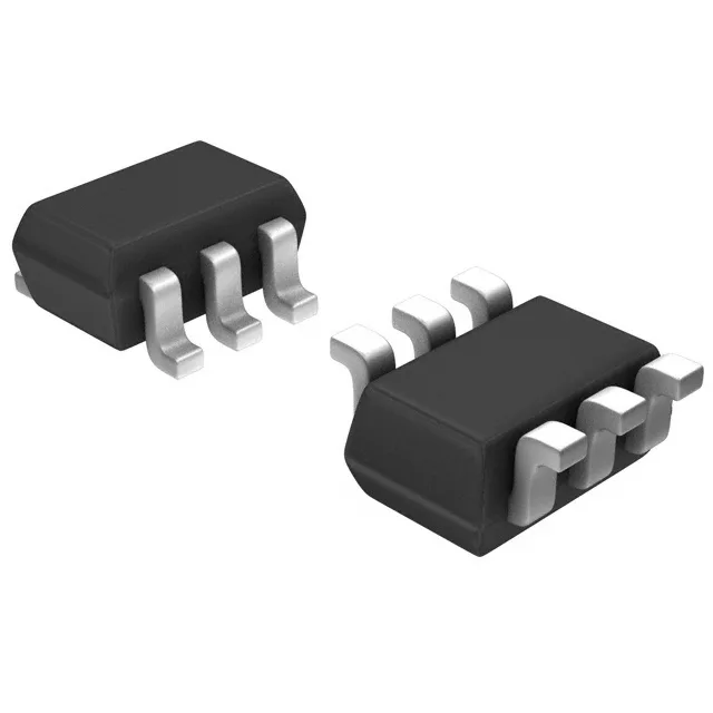
Two NPN transistors share the same SOT-363 package (6-VSSOP, SC-88, Infineon's PG-SOT363-PO). The footprint is 2.1 mm × 2.0 mm with 0.65 mm pin pitch — standard for a dual RF transistor, and the same land pattern works for the BFS483 and its siblings. Surface-mount only; the small body means the hot-air rework profile is short — 150 °C preheat for 60 seconds, then 260 °C peak for 10 seconds on the leads, and the part lifts clean. The 450 mW maximum power dissipation is shared between the two die. In practice, each transistor dissipates maybe 20–30 mW in a typical LNA stage, so the thermal margin is generous. No exposed pad — heat flows through the collector leads, so the PCB copper pour under the package matters less than for a power transistor.