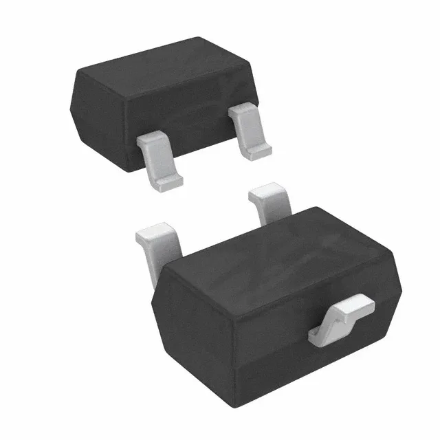
Infineon Technologies BFR182WH6327XTSA1 — Logic ICs

BFR182WH6327XTSA1 NPN RF Transistor, 8 GHz, 19 dB Gain

MPNBFR182WH6327XTSA1
End of Life

Infineon BFR182WH6327XTSA1 NPN RF transistor, 12 V VCEO, 35 mA Ic, 8 GHz fT, 19 dB gain, 0.9 dB noise figure at 900 MHz, 250 mW max power, SC-70/SOT-323 package, surface mount.

$0.41Ref. price · indicative, final on quote
PackagingSC-70, SOT-323
StockContact for availability
MOQ1 pcs
  • 100% new & originalTraceable channels only — no refurbs, no pulls, no remarked parts.
  • Date & lot codes on quoteStated per line before you commit; label photos on request.
  • MSL-compliant ESD packingMoisture-sealed bags with indicator cards; reels photo-verified.
  • PayPal buyer protectionPay by T/T, PayPal or Payoneer — card payments covered end to end.

Specifications

BFR182WH6327XTSA1 Technical Specifications
ParameterValue
Mounting typeSurface Mount
FET typeNPN
Voltage - collector emitter breakdown12V
Current - collector (Ic)35mA
DC current gain (hFE) (Min) @ ic, vce70 @ 10mA, 8V
Power - max250mW
Frequency8GHz
Operating temperature150°C (TJ)
Gain19dB
PackageTape & Reel (TR); Cut Tape (CT)
CaseSC-70, SOT-323
Noise figure (dB typ @ f)0.9dB ~ 1.3dB @ 900MHz ~ 1.8GHz

Product details

RF front-end NPN in SOT323 — 8 GHz fT, 19 dB gain

The Infineon BFR182WH6327XTSA1 is an NPN silicon RF bipolar transistor designed for low-noise amplifier and driver stages up to the low-GHz range. It delivers a typical gain of 19 dB with a transition frequency of 8 GHz, making it a fit for cellular, ISM-band, and GPS receiver front-ends. The noise figure runs 0.9 dB to 1.3 dB across 900 MHz to 1.8 GHz, which keeps the LNA noise contribution low in a 50 Ω system. Collector current is rated to 35 mA maximum, and the 12 V collector-emitter breakdown voltage gives headroom for a 3 V to 5 V supply rail with margin.

Package and mounting — SC-70 / SOT-323

Housed in a three-lead SC-70 (SOT-323) package, the BFR182WH6327XTSA1 is a surface-mount device with a small footprint — about 2.0 mm × 1.25 mm. The supplier device package is PG-SOT323. The 250 mW power dissipation limit means the part is intended for small-signal stages, not output drivers.

Temperature rating and bias conditions

The junction temperature rating goes to 150 °C, which is standard for commercial and industrial RF stages — no special derating needed for ambient up to 85 °C as long as the collector current stays within the 35 mA ceiling. The DC current gain (hFE) is specified at 70 minimum when biased at 10 mA collector current and 8 V collector-emitter voltage. That gain floor is enough for a single-stage LNA with resistive feedback; for higher gain per stage, the BFR181 sibling (also 19 dB gain) offers a similar bias point at a lower 175 mW power rating.

Frequently asked questions

Is BFR182WH6327XTSA1 obsolete or end-of-life?

For production programs this means no imminent LTB risk, though it is always prudent to check PCN status at quote time.

What is the closest functional second-source for BFR182WH6327XTSA1?

The BFR181WH6327XTSA1 is the closest functional peer — same 19 dB gain, same 8 GHz fT, same SOT323 package, but rated at 175 mW max power versus 250 mW. The BFR181 runs slightly cooler and may be preferred in power-constrained designs; otherwise the two are drop-in interchangeable for most LNA stages.