Low-noise Si NPN for receiver front-ends up to C-band
The Infineon BFP520FH6327 is a low-noise silicon NPN bipolar RF transistor designed for small-signal amplification in wireless receiver front-ends, LNA stages, and oscillator buffer chains up to several gigahertz. Its 45 GHz transition frequency (fT) and 22.5 dB gain at 1.8 GHz make it a fit for GSM, WCDMA, LTE, and ISM-band LNA designs where noise figure and gain flatness drive the cascade budget.
Noise figure and gain at 1.8 GHz — the LNA benchmark
Noise figure is specified at 0.95 dB typical at 1.8 GHz, a common reference for cellular and ISM-band LNA evaluation. The 22.5 dB gain at that same frequency means a single stage can lift a -100 dBm signal to a level the mixer or ADC can resolve without a second gain block, provided the collector supply is held at or below 2.5 V. At 50 mA maximum collector current, the part is sized for low-to-medium current LNA and driver stages, not power amplification.
Package and thermal handling for the 4-TSFP
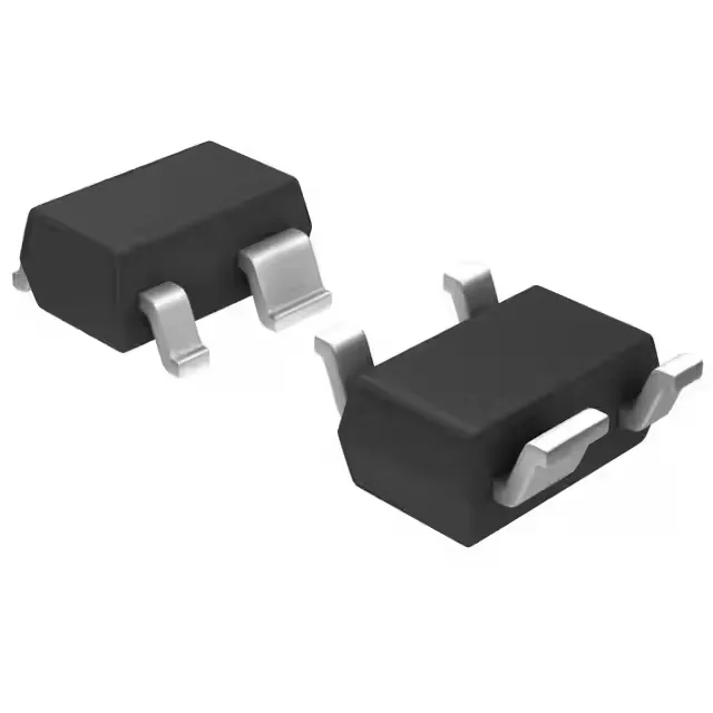
The 4-TSFP package (4-SMD with flat leads) is a small outline with a low parasitic footprint suited to RF layouts up to 45 GHz. The junction temperature rating of 150 °C and 120 mW maximum power dissipation mean the part can run warm in a dense RF section, but the thermal path relies on the PCB copper — no exposed pad. Keep the collector pad connected to a ground plane via short vias to pull heat out of the die.