RF small-signal gain and noise floor
The BFP193WH6327XTSA1 delivers 13.5 dB to 20.5 dB small-signal gain across its bias range — enough for a single-stage LNA front-end in the 900 MHz to 2.4 GHz ISM bands without cascading a second gain block. Noise figure runs 1 dB to 1.6 dB typ at 900 MHz to 1.8 GHz, so the transistor's own noise contribution stays below the thermal floor of a 50-ohm source — the cascaded receiver NF is set by the first-stage bias, not the device. Transition frequency of 8 GHz means usable gain extends past 3 GHz before the 3 dB roll-off; the part is specced for VHF/UHF through low-microwave oscillator and driver stages.
Bias design and safe operating area
Maximum collector current is 80 mA, collector-emitter breakdown is 12 V, and total power dissipation is 580 mW — bias the part at 30 mA, 8 V (the hFE test point) and you stay inside the SOA with margin for temperature derating. DC current gain is minimum 70 at 30 mA, 8 V — this gives a predictable base-drive current for bias networks; the hFE floor ensures the part does not starve the collector at the low-end of the gain curve.
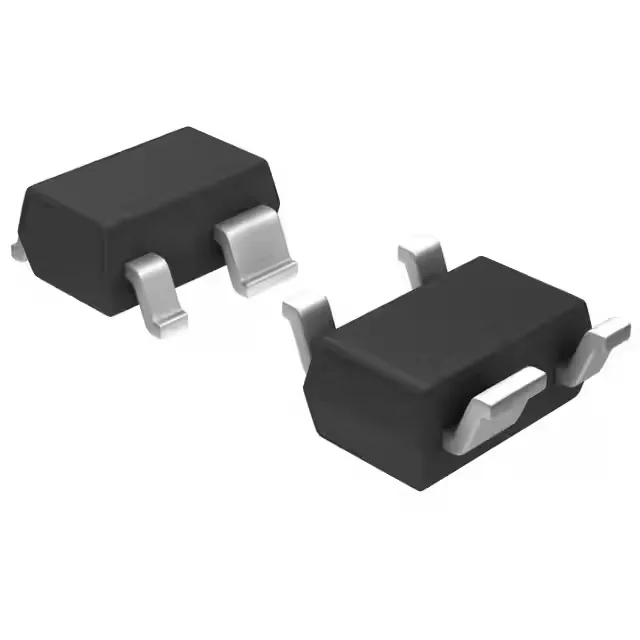
Housed in a SC-82A / SOT-343 package (Infineon code PG-SOT343-3D), the part shares the standard 4-pin footprint used by many RF transistors in this class — the collector tab on the backside requires a thermal via pattern for best heat transfer. Surface-mount assembly with tape-and-reel or cut-tape packaging; the reel quantity suits medium-volume pick-and-place without a reel change.
RoHS3 compliant (2011/65/EU + 2015/863), with no restricted substances above the threshold limits — the part ships without a compliance exemption sticker, which simplifies EU market clearance.