8.5 GHz transition frequency sets the usable band
The BFP183WH6327XTSA1 is an NPN silicon RF transistor with a transition frequency (fT) of 8.5 GHz. That figure tells you the current-gain–bandwidth product: at 900 MHz, the device still has roughly 9.4× current gain, which is enough for a single-stage LNA before the gain rolls off. Above 2.4 GHz, the available gain drops faster, so this part is most at home in the 800 MHz to 2.1 GHz cellular and ISM bands. Noise figure runs 0.9 dB typical at 900 MHz and 1.4 dB at 1.8 GHz. That spread is tight enough that the same BOM position can serve dual-band front-ends without swapping transistors. The 22 dB gain listed is at the bias point of 15 mA, 8 V — not a no-signal figure — so the actual stage gain in a 50-Ω system lands a few dB lower after matching losses.
Breakdown voltage and collector current limit the bias point
Collector-emitter breakdown is 12 V maximum, and the continuous collector current is rated 65 mA. At 65 mA and 8 V, you are at 520 mW — that exceeds the rating, so the bias network must limit Ic to about 56 mA at that Vce to stay inside the SOA. That means the base drive current for the bias network is about 215 µA — easy for a resistor divider from the supply, but the beta variation with temperature and collector current means the bias point shifts.
SOT-343 footprint and thermal path
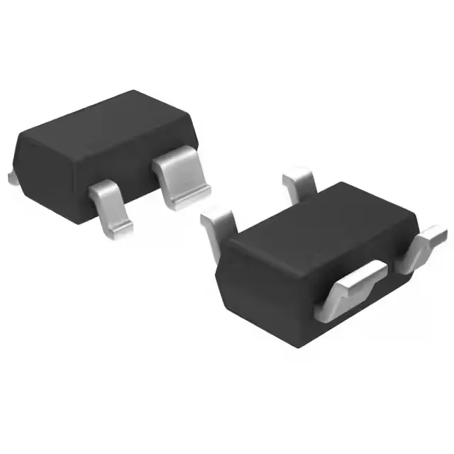
The package is SC-82A (SOT-343), Infineon's PG-SOT343-3D variant. It is a 4-pin surface-mount package with the collector on the backside paddle — the same footprint as the standard SOT-343. Without a thermal via or a ground plane under the paddle, the junction temperature rises faster than the 150°C rating allows at high bias currents. The tape-and-reel option (TR) is the production quantity; cut tape (CT) is available for prototypes and small runs. Both are ROHS3 compliant, with no exemptions that complicate EU or California market entry.