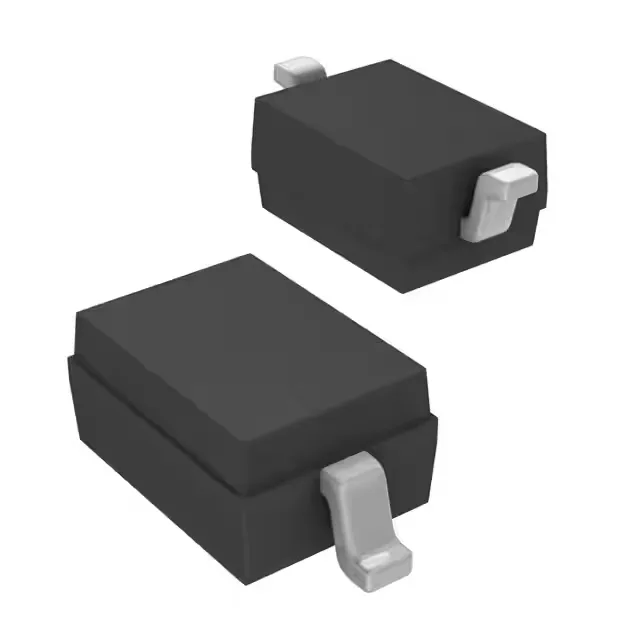
200 mA Schottky in a SOD-323 — the forward drop and recovery trade-off
The BAT5403WE6327HTSA1 is a 30 V, 200 mA Schottky rectifier in the SOD-323 (PG-SOD323-3D) package. The 800 mV forward drop at 100 mA is higher than a typical 30 V Schottky of this current class — expect around 0.45–0.55 V from a competing part — so the conduction loss is roughly 80 mW at rated current. That is the trade-off for the 5 ns reverse recovery time: the faster turn-off reduces switching losses and ringing in a 100 kHz boost converter or a flyback snubber, but the higher Vf means the diode runs warmer at steady DC. The 2 µA leakage at 25 V reverse is typical for a Schottky of this voltage class, but it doubles roughly every 10 °C junction rise. At 125 °C junction the leakage can exceed 100 µA, which matters if the diode is used in a low-power hold-up circuit or a battery-powered path where standby current is budgeted.
10 pF capacitance — the AC load it presents
The 10 pF capacitance at 1 V reverse bias and 1 MHz is the AC load the diode presents to the circuit. In an RF detector or a high-speed clamping application, this capacitance forms a low-pass filter with the source impedance — at 100 MHz, 10 pF is about 160 Ω reactance, so the diode loads the signal path. For a simple rectifier at 50/60 Hz, the capacitance is negligible. The 5 ns reverse recovery time is specified as a maximum — the actual trr depends on the forward current and the di/dt during turn-off. At 100 mA forward and a typical 100 A/µs turn-off ramp, the stored charge is small enough that the diode recovers cleanly without the snap-off ringing that plagues slower PN-junction diodes in the same package.
Active production, RoHS3, SOD-323 footprint
The base product number is BAT5403; the suffix identifies the tape-and-reel packaging and the specific SOD-323 variant. The SOD-323 footprint (SC-76) is one of the smallest packages for a 200 mA diode — the body is roughly 1.7 mm × 1.25 mm with a 0.65 mm lead pitch. The PG-SOD323-3D variant has three leads (the third is the cathode tab), so the PCB land pattern must accommodate the centre pad for thermal relief.