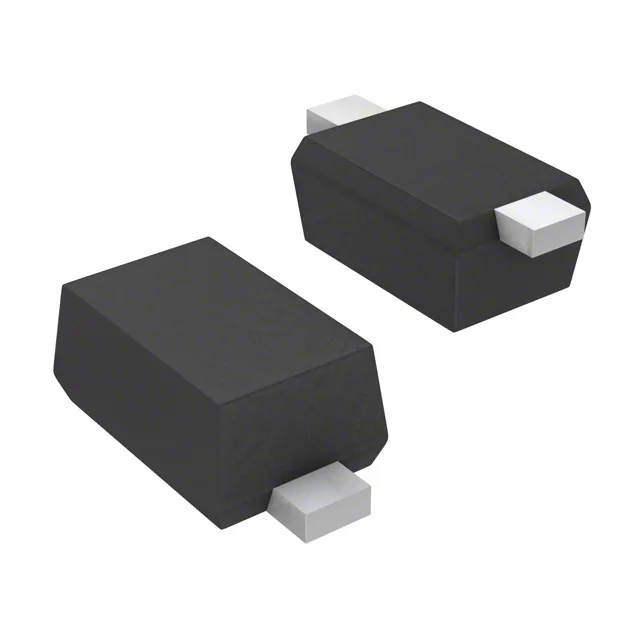
Infineon Technologies BAR6702VH6327XTSA1

Infineon BAR6702VH6327XTSA1 PIN Diode, 0.55pF, SC-79

MPNBAR6702VH6327XTSA1
End of Life

Infineon BAR6702VH6327XTSA1 single PIN diode, 150 V peak reverse, 200 mA max, 0.55 pF capacitance @ 5 V, 1 Ohm resistance @ 10 mA / 100 MHz, 250 mW, SC-79 / SOD-523 package, PG-SC79-2.

$0.43Ref. price · indicative, final on quote
PackagingSC-79, SOD-523
RoHSROHS3 Compliant
Independent supplier — new & surplus stockAuthenticity-screened · ESD-safe packingListing updated Jul 2026

Specifications

BAR6702VH6327XTSA1 specifications
ParameterValue
Diode typePIN - Single
Voltage - peak reverse150V
Current - max200 mA
Power dissipation250 mW
Operating temperature150°C (TJ)
PackageTape & Reel (TR); Cut Tape (CT)
CaseSC-79, SOD-523
Resistance @ if,1Ohm @ 10mA, 100MHz
Capacitance @ vr,0.55pF @ 5V, 1MHz

Product details

RF switch and attenuator core — 0.55 pF at 5 V

The Infineon BAR6702VH6327XTSA1 is a single PIN diode designed for RF switching and attenuator circuits up into the UHF and low-microwave bands. Its capacitance of 0.55 pF at 5 V reverse bias keeps the off-state isolation high without loading the signal path, while the series resistance of 1 Ohm at 10 mA forward current and 100 MHz gives a low insertion loss when biased on. Rated for a peak reverse voltage of 150 V and a maximum forward current of 200 mA, this diode handles the RF power levels typical of base station T/R switches, antenna diversity circuits, and variable attenuators without breaking down.

Thermal budget in a compact package

The 250 mW power dissipation limit and 150 °C junction temperature rating set the thermal ceiling for continuous RF power.

Frequently asked questions

What is the capacitance of BAR6702VH6327XTSA1 at 5V?

The capacitance is 0.55 pF at a reverse voltage of 5 V and a test frequency of 1 MHz. This low capacitance keeps the off-state isolation high in RF switching and attenuator applications.

What is the difference between a PIN diode and a Schottky diode?

A PIN diode has an intrinsic (I) layer between the P and N regions, giving it a low resistance under forward bias and a low capacitance under reverse bias — ideal for RF switching and attenuation. A Schottky diode uses a metal-semiconductor junction for fast switching and a lower forward voltage drop, but it lacks the PIN's low-capacitance RF performance at higher frequencies.