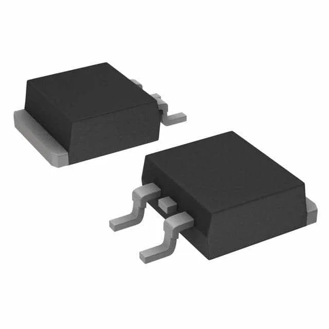
650 V / 55 A Trench Field Stop IGBT in D2Pak
The Infineon AIKB30N65DF5ATMA1 is a 650 V, 55 A Trench Field Stop IGBT in a surface-mount TO-263-3 (D2Pak) package. This is the part a power-stage designer reaches for when they need a 650 V blocking voltage, 55 A continuous collector current, and the low saturation voltage of a Trench Field Stop structure — typically in motor drives, uninterruptible power supplies, welding inverters, and PFC stages where the bus runs at 400 VDC. The 188 W power dissipation ceiling and 175 °C maximum junction temperature give the thermal budget for continuous hard-switched operation in an industrial environment.
70 nC gate charge — sizing the driver
The 70 nC total gate charge at 15 V drive is the number that sizes the gate-driver output stage and the bootstrap supply. For a 55 A IGBT this is a moderate Qg — a typical 2 A peak-drive gate-driver IC will switch it cleanly at 20–40 kHz. The turn-on delay of 25 ns and turn-off delay of 188 ns (at 25 °C, 400 V, 15 A, 23 Ω gate resistor) are the timing numbers to plug into the loss calculation spreadsheet.
Switching energy and reverse recovery
At the test condition of 400 V, 15 A, 23 Ω gate resistor, and 15 V gate drive, the part dissipates 330 µJ during turn-on and 100 µJ during turn-off. The co-packaged diode recovers in 67 ns — fast enough to keep the shoot-through current and EMI under control in a half-bridge leg. These numbers let you estimate the switching loss contribution before you get to the bench.
For volume pricing and lead time, submit an RFQ — we source this line and will quote against your BOM quantity.