What the 2EDL8024GXUMA1 does in a power stage
The Infineon 2EDL8024GXUMA1 is a high-side and low-side gate driver from the EiceDriver™ family, designed to drive N-channel MOSFETs in half-bridge and full-bridge topologies. It provides independent drive channels with a peak output current of 4A source and 4A sink, making it suitable for switching power supplies, motor drives, and DC-DC converters where the power-stage bus voltage stays under 90 V (the bootstrap high-side maximum). The supply range of 8 V to 17 V aligns with standard 12 V bias rails, and the operating junction temperature of -40°C to 125°C covers industrial and automotive under-hood environments.
4A peak drive — what it means for gate charge
The 4A source and sink peak current rating determines how fast the driver can charge and discharge the MOSFET gate capacitance. With a typical rise and fall time of 45 ns, this driver can handle moderate gate charges — think a few tens of nC — without excessive switching losses. If your MOSFET has a gate charge above 100 nC, the effective switching speed will be slower than the 45 ns figure suggests; check the gate charge curve against the driver's output resistance to confirm the actual transition time. The independent channel architecture lets you adjust the gate drive strength per device by adding external gate resistors on each output.
Bootstrap operation and high-side voltage ceiling
The high-side driver is bootstrapped, with a maximum high-side voltage of 90 V. This means the floating supply for the high-side gate drive is generated by a bootstrap diode and capacitor from the low-side supply rail. The 90 V ceiling sets the absolute maximum DC bus voltage the power stage can run — design the bus rail with margin below 90 V, and account for switching transients that could push the bootstrap node higher. The bootstrap capacitor should be sized per the app note guidelines; a typical value for this driver class is 100 nF to 1 µF, depending on the gate charge and switching frequency.
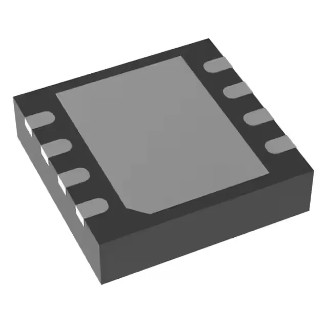
The 2EDL8024GXUMA1 comes in an 8-VDFN exposed-pad package, supplier device code PG-VDSON-8-4. The non-inverting input type means the output follows the input logic level without inversion, simplifying the control interface from the PWM controller or MCU.
The 2EDL8024GXUMA1 remains the correct choice for the 4 A peak, 90 V bootstrap, 8-VDFN footprint.