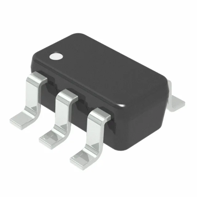
Infineon Technologies 1EDN7550BXTSA1 — Discrete Semiconductors

Infineon 1EDN7550BXTSA1 EiceDriver, 4A/8A peak, SOT-23-6

MPN1EDN7550BXTSA1
End of Life

Infineon Technologies EiceDriver™ series, single high-side gate driver, 1EDN7550BXTSA1, 4A source / 8A sink peak output, 6.5ns rise / 4.5ns fall, SOT-23-6 package, -40°C to 150°C.

$0.94Ref. price · indicative, final on quote
PackagingSOT-23-6
StockContact for availability
Lead timeIn Stock wk
MOQ1 pcs
  • 100% new & originalTraceable channels only — no refurbs, no pulls, no remarked parts.
  • Date & lot codes on quoteStated per line before you commit; label photos on request.
  • MSL-compliant ESD packingMoisture-sealed bags with indicator cards; reels photo-verified.
  • PayPal buyer protectionPay by T/T, PayPal or Payoneer — card payments covered end to end.

Specifications

1EDN7550BXTSA1 Technical Specifications
ParameterValue
SeriesEiceDriver™
Gate typeN-Channel, P-Channel MOSFET
Input typeNon-Inverting
Channel typeSingle
Mounting typeSurface Mount
Voltage4.5V ~ 20V
High side voltage - max (Bootstrap)84 V
Current - peak output (Source, sink)4A, 8A
Operating temperature-40°C ~ 150°C (TJ)
PackageTape & Reel (TR); Cut Tape (CT)
CaseSOT-23-6
Number of drivers1
Driven configurationHigh-Side
Rise (Fall time)6.5ns, 4.5ns

Product details

The 1EDN7550BXTSA1 is supplied in a PG-SOT23-6 package (SOT-23-6), a 6-lead surface-mount footprint with a 0.95 mm pitch typical for this class. The small body — roughly 2.9 mm × 1.6 mm — places the driver close to the MOSFET gate loop, minimising parasitic inductance in the drive path. The exposed die attach pad on the PG variant improves thermal conduction to the board; a thermal via under the pad to the ground plane is recommended for high-frequency switching above 500 kHz.

Peak current and switching speed

Rated for 4 A peak source and 8 A peak sink output current, this driver can charge and discharge the gate capacitance of medium-power N-channel and P-channel MOSFETs quickly. The 6.5 ns typical rise time and 4.5 ns typical fall time (into a specified load) set the switching loss ceiling — faster edges reduce cross-conduction losses in the half-bridge but increase EMI, so the board layout must keep the gate loop inductance below 10 nH to avoid ringing.

Supply rail and bootstrap voltage

The high-side bootstrap pin is rated to 84 V maximum, allowing the driver to float on the switching node of a half-bridge with a DC-link voltage up to 80 V. This makes the part suitable for 48 V bus converters, 60 V motor pre-drives, and 72 V battery-powered systems where the bootstrap diode and capacitor must be sized for the full rail voltage.

Specified for operation from -40°C to 150°C junction temperature, the 1EDN7550BXTSA1 meets the thermal requirements for under-hood automotive electronics and industrial motor drives that see sustained ambient temperatures above 85°C.

Frequently asked questions

What is the peak output current rating of 1EDN7550BXTSA1?

The driver is rated for 4 A peak source and 8 A peak sink output current, enabling fast charging and discharging of the MOSFET gate capacitance.

What supply voltage range does 1EDN7550BXTSA1 support?

The bootstrap pin is rated to 84 V maximum.

What package is 1EDN7550BXTSA1 available in?

The part is supplied in a PG-SOT23-6 surface-mount package (SOT-23-6), a 6-lead footprint approximately 2.9 mm × 1.6 mm.