4 MB flash, 536 KB SRAM — the memory budget for a connected edge node
The ESP32-MINI-1U-H4 carries 4 MB of embedded flash, 448 kB of ROM, and 536 kB of SRAM on the ESP32-U4WDH die. For a typical IoT application running an RTOS with a WiFi stack and TLS, the SRAM leaves roughly 200–250 kB free for the application heap after the protocol buffers and the Bluetooth controller are allocated — enough for a JSON parser and a modest sensor buffer without external PSRAM. The 4 MB flash is the same footprint used by Espressif's ESP-IDF OTA example — a full application image plus a fallback partition fits within 2 MB, leaving the other half for a second-stage bootloader and a small file system. If your firmware image exceeds 3 MB, you will need to compress the partition table or move to a module with external flash.
Dual-protocol radio: 802.11b/g/n at 150 Mbps plus Bluetooth v4.2
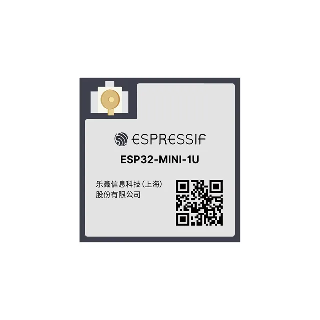
The radio covers 2.4 GHz WiFi at a data rate of 150 Mbps and Bluetooth v4.2 with EDR, supporting Class 1, 2, and 3 transmit power levels. The 19.5 dBm max output power means the module can push a usable signal through two interior walls in a residential setting — the link budget at -97 dBm sensitivity gives roughly 116 dB of path loss margin at 1 Mbps, which translates to about 50–60 meters line-of-sight with the on-board trace antenna (antenna not included in this variant; the U.FL connector expects an external antenna). Modulation includes 8DPSK and DQPSK for Bluetooth, and the standard OFDM/CCK for WiFi. The module handles concurrent WiFi and Bluetooth operation via a shared antenna port — the coexistence algorithm in the ESP32 firmware arbitrates the RF front-end, so a BLE beacon scan does not drop the WiFi association as long as the beacon interval is above 100 ms.
Active production — no last-time-buy window to manage
For a BOM that requires a second-source hedge, the ESP32-MINI-1U-H4 shares the same footprint and pinout as the ESP32-MINI-1U (non-H4 variant) — the difference is the flash die inside. The H4 suffix indicates a specific flash vendor and temperature grade; swapping to the base variant requires firmware re-validation of the flash timing parameters but no board spin.
The 105°C ceiling puts it in the industrial-plus band — suitable for outdoor enclosures, engine-bay-adjacent telematics, or a sealed IoT gateway that sees solar loading. At 105°C the internal regulator's dropout margin shrinks; the 3 V minimum supply must be held within ±2% at the module pin, not at the board input. Current consumption during receive is 112–118 mA; during transmit it ranges from 260 mA to 379 mA depending on the output power setting and the protocol in use. A 3.3 V rail feeding the module should be rated for at least 500 mA to cover the peak transmit current plus the inrush from the on-chip buck converter's startup sequence.
55-SMD module — reflow profile and antenna routing
The package is a 55-SMD module, surface-mount, with a castellated edge for the RF and I/O pads. The land pattern is a standard 0.8 mm pitch; the module's own PCB substrate has a ground plane underneath the ESP32 die, so the board-level ground pour should extend at least 3 mm beyond the module footprint to maintain the RF reference plane. The U.FL connector sits on the module edge — keep the 50-ohm trace from the connector to the antenna feed point as short as possible, ideally under 10 mm, to minimise insertion loss.