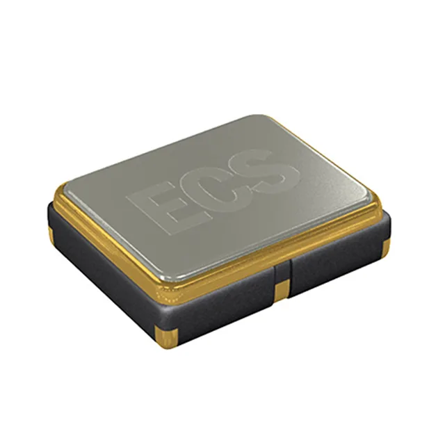
MultiVolt supply — one part, two rail voltages
The ECS-2520SMV-270-FP-TR: The 1.62–3.63 V supply window spans the two most common MCU and SoC clock rails without requiring separate XO variants for 1.8 V and 3.3 V designs — a single part number covers both boards on a product family, simplifying BOM consolidation and reducing the risk of a wrong-frequency part slipping into the wrong build. The Enable/Disable pin further sharpens this advantage in systems that gate clocks to save power during low-power or standby states.
±10 ppm stability across the industrial thermal band
Frequency stability of ±10 ppm at 27 MHz translates to a maximum deviation of ±270 Hz across the operating range — tight enough for UART clocking, SPI timing, and USB fractional-N synthesis without requiring software compensation. The -40 °C to 105 °C grade places this squarely in the industrial and light automotive temperature envelope; a design targeting under-hood or factory-floor environments stays within the ±10 ppm band without additional thermal management. Compare this against a ±20 ppm or ±50 ppm XO, where the accumulated timing error on a 1 ppm-synthesis UART clock demands a more forgiving baud-rate tolerance or a firmware trim table.
Board footprint and disable-current sanity check
Maximum supply current is 10 mA, which sets the minimum decoupling capacitance at the VCO rail — a single 100 nF ceramic placed close to the supply pin handles the high-frequency switching transient of the HCMOS output stage. In disable mode the oscillator draws a maximum of 10 µA, confirming it is safe to leave the supply rail active on µC boards that enter deep-sleep and gate the Enable line rather than remove power entirely.