Active production — still a valid BOM line for mil/aero
The OP02EZ: RoHS non-compliant — the internal die attach and lead finish use tin-lead solder. This is a deliberate feature for defense and aerospace assemblies that require tin-whisker mitigation per MIL-STD-1580 or NASA-STD-6016.
Hermetic CERDIP package for sealed-environment reliability
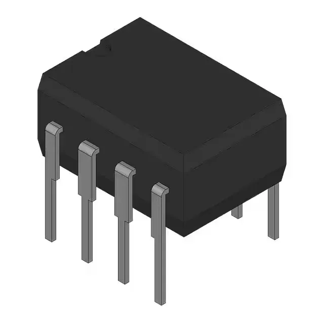
Housed in an 8-CERDIP (ceramic dual-in-line) package with a 0.300-inch body width and 7.62 mm row spacing. The hermetic ceramic-and-glass seal keeps moisture and contaminants out — this is the package choice for vacuum systems, high-altitude avionics, and downhole logging tools where plastic SOIC packages would fail from outgassing or moisture ingress. Through-hole mounting — the leads are tin-lead plated and solder to standard 0.100-inch pitch plated-through holes. No reflow profile needed; hand solder or wave solder with a 260°C peak tip temperature.
Military temperature range and supply flexibility
Rated for -55°C to +125°C operating ambient — the full military temperature band. This is not an industrial-grade part with a commercial temp range; it is screened for the thermal extremes of engine-bay electronics, satellite thermal cycling, and arctic deployment. Supply span from 10 V to 44 V — runs on standard ±15 V bipolar rails or a single 24 V industrial supply without an extra regulator. The wide compliance voltage also suits it for 28 V aircraft bus applications.
Parametric performance for precision signal conditioning
Gain-bandwidth product of 1.3 MHz with a 0.5 V/µs slew rate. For a closed-loop gain of 10, the small-signal bandwidth is about 130 kHz — adequate for transducer amplification, thermocouple conditioning, and servo loop compensation in motion control. Input offset voltage trimmed to 1 mV typical, with 1 nA input bias current. These figures mean the OP02EZ can resolve microvolt-level signals without external nulling in many bridge and strain-gauge circuits. Single-channel (one op-amp per package) in the 8-pin CERDIP. The pinout is the standard dual-in-line op-amp arrangement — offset null pins 1 and 5, inverting input pin 2, non-inverting input pin 3, V- pin 4, output pin 6, V+ pin 7, NC pin 8.