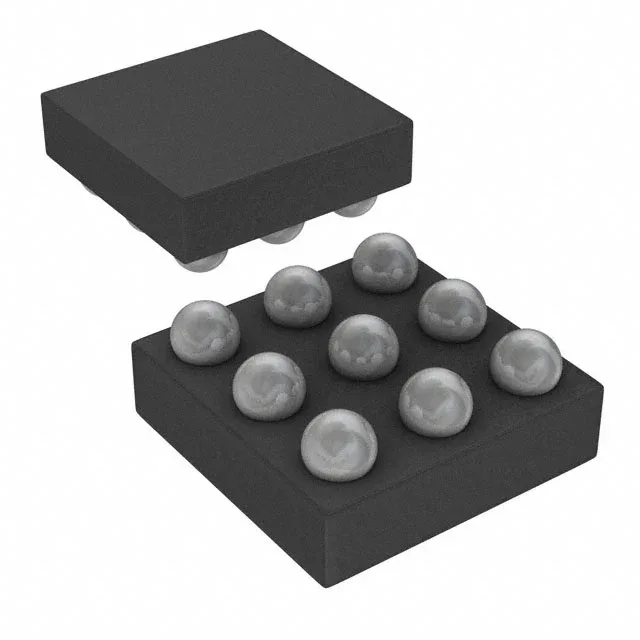
Boost converter with a fixed 3.7 V rail
The MAX8969EWL37+T: It is a single-output, positive-configuration boost with a 700 mA current capability and synchronous rectification built in, so no external Schottky catch diode is needed on the BOM. The 3 MHz switching frequency allows the use of small-value inductors and ceramic output capacitors, shrinking the total solution footprint — useful when board real estate is tight. The synchronous rectifier improves efficiency at light loads, which matters for battery-powered applications where the load idles between active bursts.
Input and output voltage boundaries
The input voltage range spans 2.5 V (minimum) to 5.5 V (maximum). This covers a single-cell lithium-ion battery (3.0 V to 4.2 V nominal) and a 5 V USB rail. The fixed output of 3.7 V is a typical Li-ion battery charge termination voltage or a post-regulation rail for a 3.3 V system with headroom for a linear regulator. The output current rating of 700 mA is the peak switch current limit, not the continuous load — the achievable output current depends on the input-to-output voltage ratio and inductor ripple. At a 3.0 V input and 3.7 V output, the continuous load capability is lower than 700 mA; the datasheet's efficiency curves give the real derating. This suits outdoor IoT gateways, automotive cabin electronics, and factory-floor sensor nodes that see ambient temperature swings but not under-hood extremes.
9-WLP package and board integration
The MAX8969EWL37+T is supplied in a 9-bump WLP (Wafer-Level Package) measuring 1.26 mm × 1.26 mm (: 9-WLP). The 0.4 mm pitch bumps require a solder-mask-defined pad on the PCB. The small footprint is the primary advantage — the converter and its passives fit in a corner of a multi-layer board. Surface-mount assembly with standard reflow profiles. Available in Tape & Reel (TR) for production pick-and-place or Cut Tape (CT) for prototype builds. No through-hole step.