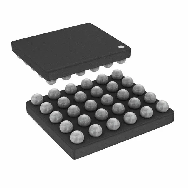
What the MAX77659AENV+ packs into that 30-WLP
The MAX77659AENV+ is a single PMIC from Analog Devices that integrates a 1-cell Li-Ion/Polymer battery charger with three buck-boost outputs, all managed over an I²C interface. The scorch mark on a dead board rarely lands on a PMIC this dense — but when it does, you want to know exactly what you are swapping. Charger side: constant-current programmable up to 300 mA max, battery pack voltage capped at 4.6V max, with programmable current, timer, and voltage. Supply input max is 5.5V. That 300 mA ceiling tells you this is sized for a wearable or IoT sensor battery, not a tablet — the charge current is the bottleneck if you try to push it into a larger cell. The 30-WLP package (2.37x2.55 mm) is a fine-pitch BGA — the board layout engineer needs to plan for thermal vias under the exposed pad and keep the I²C traces short to avoid bus capacitance issues.
Package reality for the rework bench
Supplied in Strip form, the 30-WLP is a wafer-level package with no molded body — the die backside is the top of the package. That means the usual rework trick of hot-air from the top needs a preheat plate underneath, or the die cracks before the balls reflow. The supplier device package dimension 2.37x2.55 mm is the footprint the PCB layout sees; the ball pitch is fine enough that a 0.35 mm stencil is the minimum for a reliable solder joint. ROHS3 compliant — no lead in the solder balls, so the reflow profile follows J-STD-020 for SAC305. The absence of a molded compound means moisture sensitivity level is typically MSL 1 for WLP, but verify the specific lot date code if the strip has been sitting on the shelf.
Active lifecycle and what that means for your BOM
For a BOM cost engineer, this means no single-source risk from obsolescence in the near term — but the WLP package and the specific charger voltage (4.6V max) limit drop-in alternatives. If the board spins, the I²C register map is the lock-in; a different PMIC means firmware changes. No stock-holding claim — the strip quantity per reel is confirmed per order.