1.8 V fixed output with precision guardbands
The MAX6068BEUR-T: For a 1.8 V rail, ±0.39% is about ±7 mV at 25°C — tight enough to bias a low-voltage ADC reference input without external trimming. Output current is rated at 5 mA, and the device draws 125 µA from the input supply — the quiescent current is well below the output drive capability, so the load regulation is dominated by the output impedance at DC. Input voltage range spans 2.5 V to 12.6 V, giving 700 mV minimum headroom above the 1.8 V output — enough to keep the pass element in regulation even with supply ripple.
Noise floor for analog signal chains
At 22 µVp-p, this reference supports a 12-bit ADC with a 1.8 V full-scale without the reference noise dominating the LSB.
SOT-23-3 package and board fit
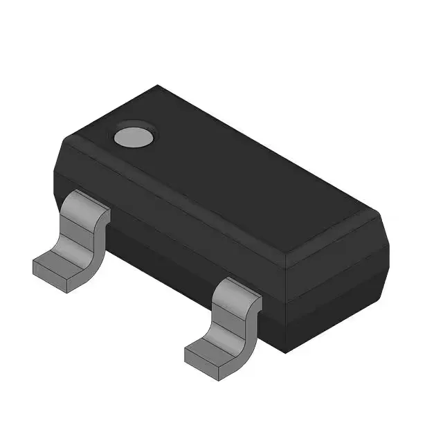
Housed in a three-pin SOT-23-3 package (also known as TO-236-3 or SC-59), the MAX6068BEUR-T occupies roughly 3 mm × 1.5 mm of board area. The pinout is input, ground, output — no external resistor divider or compensation capacitor is needed for a series reference. The small footprint lets it sit close to the load or ADC reference pin, minimising IR drops and noise pickup on the output trace.
RoHS compliance flag — plan accordingly
This part is listed as RoHS non-compliant. For BOMs that require RoHS conformance, a lead-free alternative from the same family or a different supplier should be evaluated.