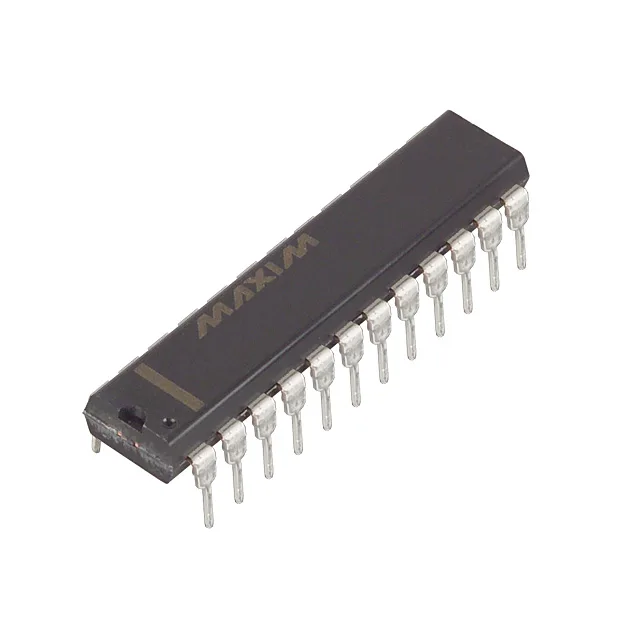
Analog Devices MAX502BCNG+ — Logic ICs

MAX502BCNG+ 12-Bit DAC, 5µs Settling, Voltage-Out, DIP-24

MPNMAX502BCNG+
End of Life

Maxim MAX502BCNG+, 12-bit voltage-output DAC, R-2R architecture, parallel data interface, 5µs settling time, ±1 LSB INL/DNL, external reference, ±11.4V to ±15.75V analog supply, 0°C to 70°C, 24-pin DIP (0.300"), Tube.

$19.13Ref. price · indicative, final on quote
Packaging24-DIP (0.300", 7.62mm)
RoHSROHS3 Compliant
Sourced new & surplus through independent channelsAuthenticity-screened · ESD-safe packingListing updated Aug 2026

Specifications

MAX502BCNG+ specifications
ParameterValue
Output typeVoltage - Buffered
MountingThrough Hole
Reference typeExternal
Voltage - supply, analog±11.4V ~ 15.75V
InterfaceParallel
Operating temperature0°C ~ 70°C
PackageTube
ArchitectureR-2R
INL (DNL)±1 (Max), ±1 (Max)
Settling time5µs
Number of bits12
Case24-DIP (0.300\", 7.62mm)
Differential outputNo
Number of d (A converters)1

Product details

12-bit voltage-output DAC in a through-hole DIP

The Maxim MAX502BCNG+ is a 12-bit digital-to-analog converter with a voltage-buffered output, built around an R-2R ladder architecture. It accepts parallel digital data and converts it to an analog voltage with a settling time of 5 µs to within 1 LSB.

A 5 µs settling time to ±1 LSB means this DAC can update its output at rates up to roughly 200 kSPS in a single-channel system, assuming the parallel bus and external reference settle within the same window. For control-loop or arbitrary-waveform applications, that settling time sets the minimum update period; a 5 µs window leaves margin for the op-amp and filter that follow. If your system needs faster updates — say 1 MSPS or above — you would look at a current-output or segmented DAC with a sub-microsecond settling spec.

±1 LSB INL/DNL — monotonicity without trimming

That means the DAC is monotonic — every digital code produces a unique analog output — and the linearity error stays within one least-significant bit. For a 12-bit system with a 10 V output span, ±1 LSB corresponds to ±2.44 mV of absolute error at the output pin, before any external reference or buffer drift. This is a production-grade spec; you do not need to trim or calibrate each board for linearity.

Frequently asked questions

What is the settling time of MAX502BCNG+?

The settling time is 5 µs to within ±1 LSB for a full-scale step, specified over the operating temperature range.

Does MAX502BCNG+ require an external reference?

Yes, the MAX502BCNG+ uses an external voltage reference (Reference Type: External). The reference input sets the full-scale output voltage and must be provided by the system.

What is the closest pin-compatible alternative to MAX502BCNG+?

Within the same Maxim family, the MAX502BCNG+ is a specific 12-bit, voltage-output, parallel-interface DAC in a 24-pin DIP. Pin-compatible alternatives would share the same package and pinout; check the Maxim DAC selector guide for devices with the same footprint and interface.